Method of forming solder bump with reduced surface defects

a technology of surface defects and solder bumps, which is applied in the direction of semiconductor devices, semiconductor/solid-state device details, electrical apparatus, etc., to achieve the effect of reducing yield and reducing bump quality

Inactive Publication Date: 2005-07-28
SAMSUNG ELECTRONICS CO LTD
View PDF4 Cites 25 Cited by
  • Summary
  • Abstract
  • Description
  • Claims
  • Application Information

AI Technical Summary

Benefits of technology

[0012] Exemplary embodiments of the present invention provide a method of forming a solder bump in which a decline in bump quality and/or

Problems solved by technology

The UBM layer may be removed without using an UBM la

Method used


Image

  • Method of forming solder bump with reduced surface defects
  • Method of forming solder bump with reduced surface defects
  • Method of forming solder bump with reduced surface defects

Examples


Embodiment Construction

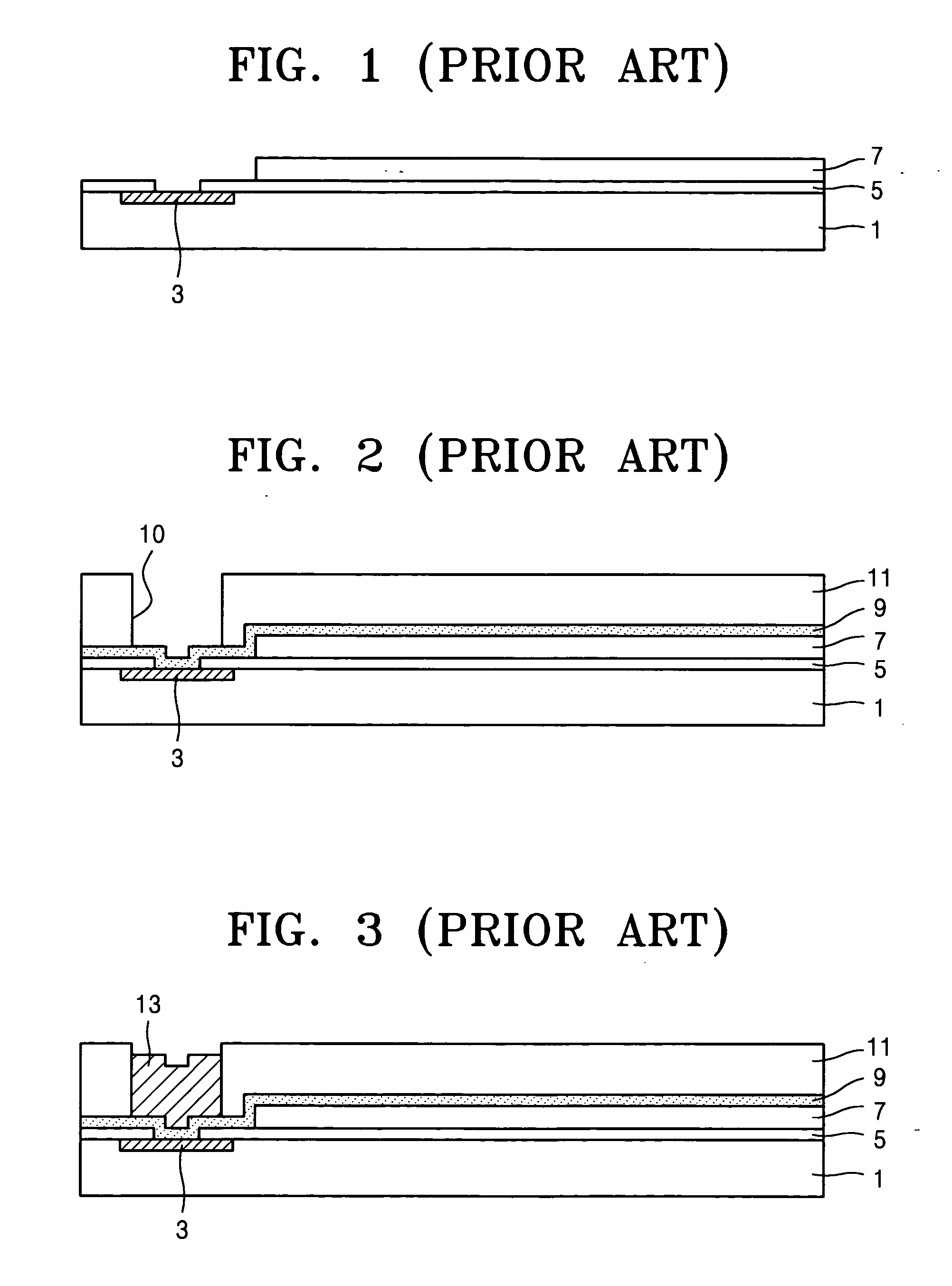
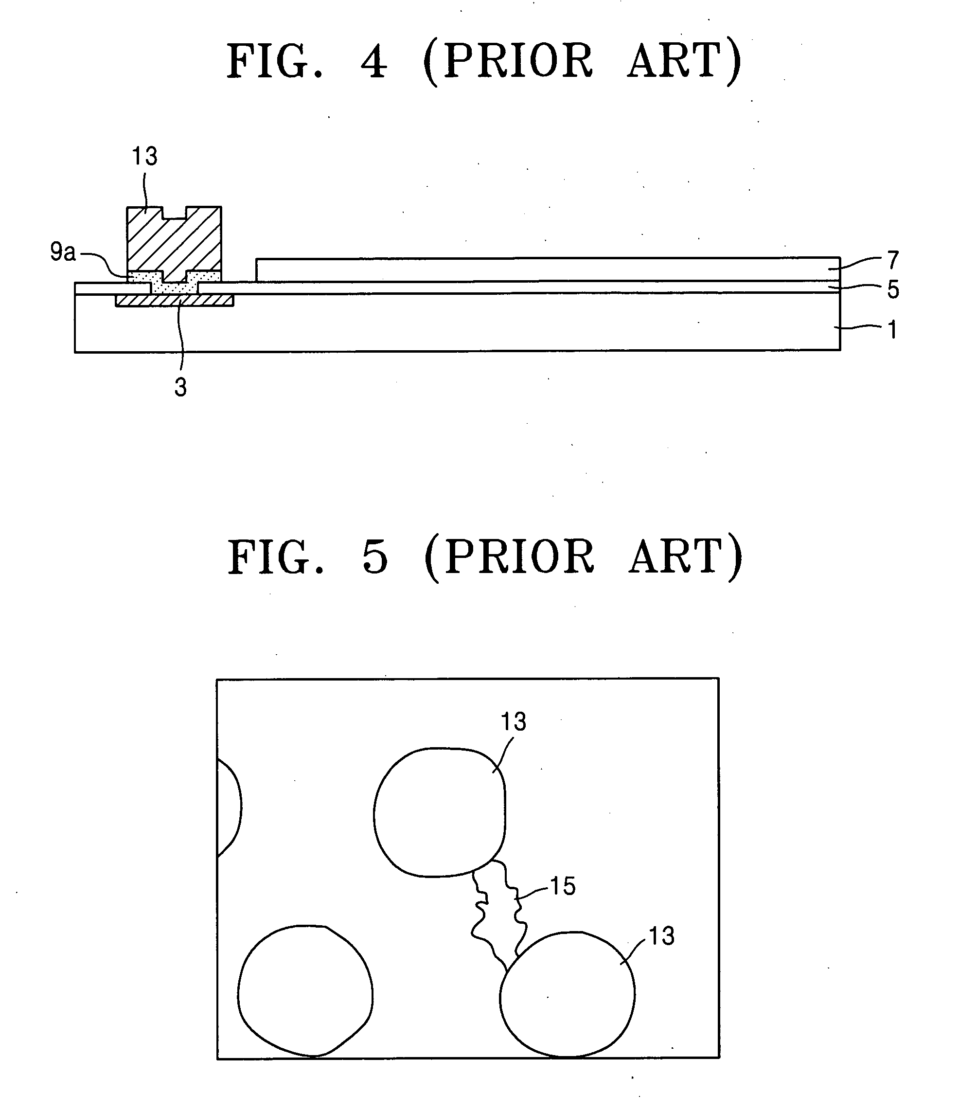
[0025] Exemplary embodiments of the present invention will now be described more fully with reference to the attached drawings. This invention may, however, be embodied in many different forms and should not be construed as being limited to the embodiments set forth herein. Rather, these embodiments are provided so that this disclosure will be thorough and complete, and will fully convey the concept of the invention to those skilled in the art.

[0026] It is to be appreciated that the figures are not drawn to scale. Rather, for simplicity and clarity of illustration, the dimensions of some of the elements are exaggerated relative to other elements. Identical reference numerals are used for like elements throughout the figures.

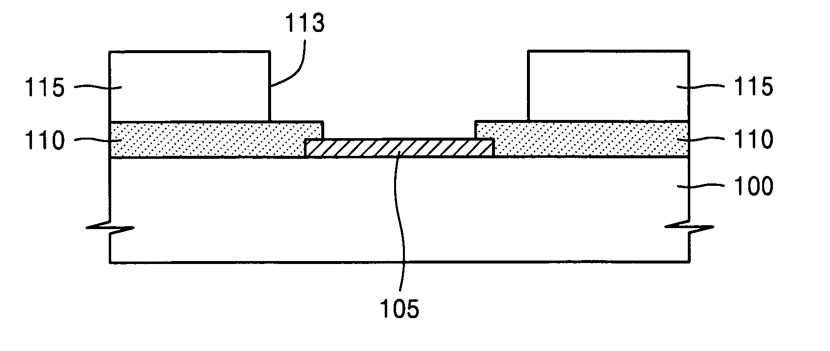
[0027] The present invention may be applied to a semiconductor chip (e.g., a silicon wafer) and / or to a carrier (e.g., a substrate such as a silicon wafer or an alumina plate) to which the semiconductor chip may be attached. That is, when connecting the semicon...


PUM


Abstract

A method of forming a solder bump may involve forming a first photoresist pattern on a wafer having a pad. The first photoresist pattern may have an opening that exposes a portion of the pad. A first under bump metallurgy (UBM) layer may be formed on the pad, and a second UBM layer may be formed on the first photoresist pattern. A second photoresist pattern may be formed that exposes the first UBM layer and covers the second UBM layer. A solder bump may be formed in the opening. The second photoresist pattern and the first photoresist pattern may be removed using a stripper, thereby removing the second UBM layer by a lift-off method.

Description

[0001] This application claims priority under 35 U.S.C. §119 to Korean Patent Application No. 2003-58003, filed on Aug. 21, 2003, in the Korean Intellectual Property Office, the disclosure of which is incorporated herein in its entirety by reference. BACKGROUND OF THE INVENTION [0002] 1. Field of the Invention [0003] The present invention relates generally to a method of forming a flip chip solder bump that may be used for connecting flip chips of semiconductor goods, and more particularly, to a method of forming the flip chip solder bump without defects on a surface of a wafer or the solder bump. [0004] 2. Description of the Related Art [0005] Three methods of connecting a chip to a carrier are wire bonding, tape automated bonding (TAB), and using a flip chip connection. Solder bumps may be formed on a wafer or the carrier to electrically connect the chip to the carrier using the TAB and the flip chip connection methods. [0006] According to conventional wisdom, an under bump metall...

Claims


Application Information

Patent Timeline
IPC IPC(8): H01L21/44H01L21/50H01L21/60H01L23/485
CPCH01L24/02H01L24/11H01L2924/0002H01L24/12H01L2224/1147H01L2224/13099H01L2924/01013H01L2924/01022H01L2924/01029H01L2924/0104H01L2924/01046H01L2924/01047H01L2924/01051H01L2924/01075H01L2924/01079H01L2924/01082H01L2924/01005H01L2924/01006H01L2924/01024H01L2924/01033H01L2924/014H01L2224/05572Y10S438/951H01L2224/0401H01L2224/05552H01L24/03H01L24/05H01L24/13H01L2224/0347H01L2224/11474H01L2924/12042H01L2924/00H01L21/60
Inventor JEONG, SE-YOUNGCHOI, JIN-HAKKIM, NAM-SEOGLEE, KANG-WOOK
Owner SAMSUNG ELECTRONICS CO LTD
Why Eureka
Try Eureka