Selector circuit and semiconductor device

a selector circuit and semiconductor technology, applied in the field of selector circuits and semiconductor devices, can solve the problems of delay in outputting selection control signals, etc., and achieve the effect of lowering the operation speed of selector circuits

Inactive Publication Date: 2005-07-28
FUJITSU LTD
View PDF0 Cites 1 Cited by
  • Summary
  • Abstract
  • Description
  • Claims
  • Application Information

AI Technical Summary

Benefits of technology

[0025] In the same manner as described for the selector circuits according to the first to third conventional examples, the selector circuit 81 according to the fourth conventional example also has the problem of having an influence on the operation of a subsequent circuit, which uses an output of the selector circuit 81. Further, a gate delay or a wiring delay described above lowers the operation speed of the selector circuit.

Problems solved by technology

A problem here is that a gate delay in the EOR circuit 83 and in the latch circuit unit 84 causes a delay in outputting the selection control signal sel.
A wiring delay of a signal line connecting the cells also causes a delay in outputting the selection control signal sel.
As a result, the timing at which the selection control signal sel transits is delayed.
Further, such a gate delay or a wiring delay may conventionally cause a defect in propagation of the selection signal S when, for example, an interval between the falling edge of the second data input signal IN2 and the rising edge of the first data input signal IN1 is narrow (a dashed line for the signal IN2 in FIG. 8).

Method used


Image

  • Selector circuit and semiconductor device
  • Selector circuit and semiconductor device
  • Selector circuit and semiconductor device

Examples


Embodiment Construction

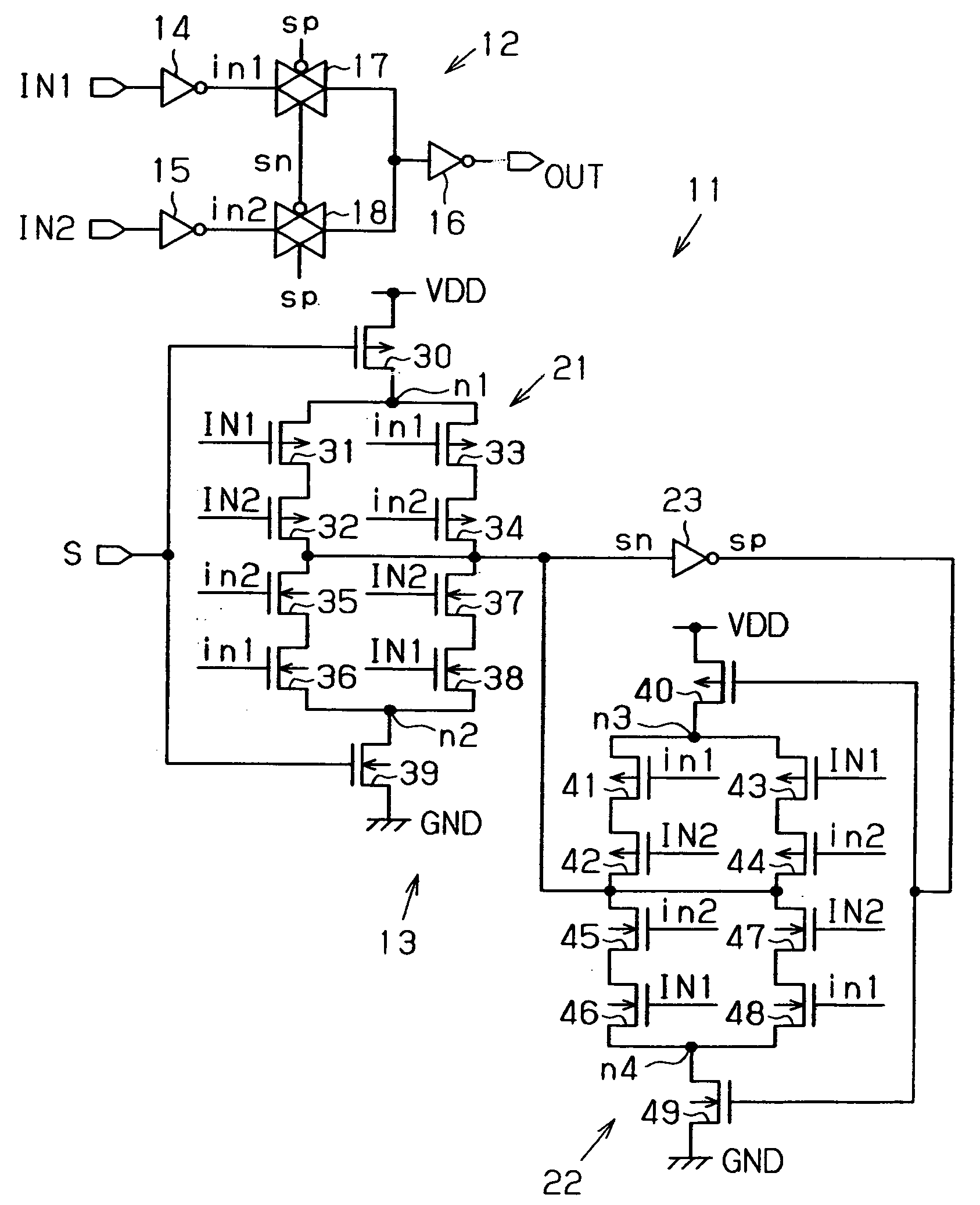
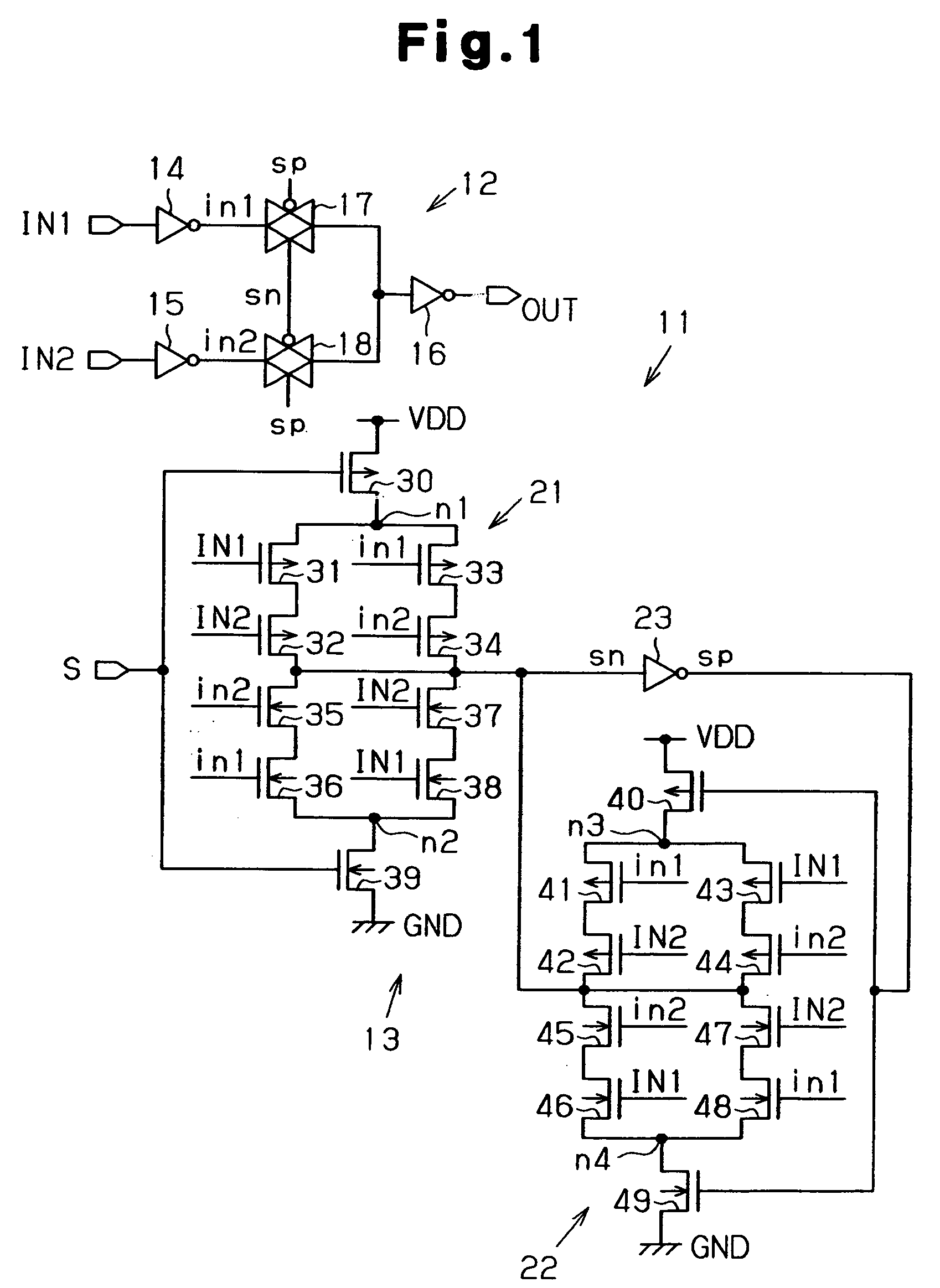
[0038] The following describes a selector circuit to be mounted on a semiconductor device, as a preferred embodiment of the present invention, with reference to FIGS. 1 and 2.

[0039]FIG. 1 is a circuit diagram showing a selector circuit according to one embodiment of the present embodiment.

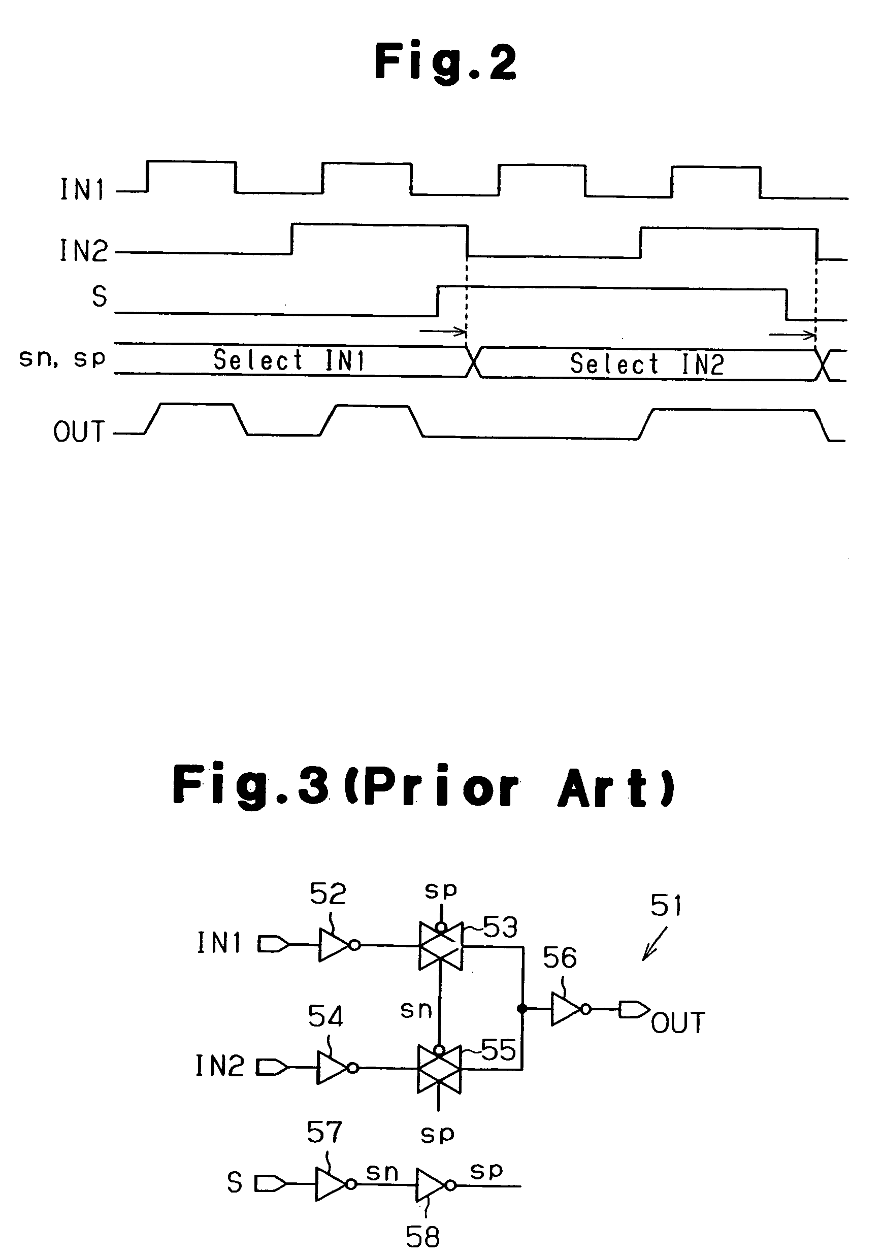
[0040] The selector circuit 11 includes a selector circuit unit 12, which selects one of first and second data input signals IN1 and IN2 according to an externally input selection signal S and outputs the selected signal, and a latch circuit unit 13, which generates first and second internal selection control signals (hereafter referred to as “internal selection signals”) sn and sp based on the selection signal S.

[0041] The selector circuit unit 12 is formed by inverter circuits 14 to 16, and first and second transfer gates 17 and 18. Each of the transfer gates 17 and 18 is formed by, for example, connecting a PMOS transistor and an NMOS transistor (not shown) in parallel.

[0042] An inversion si...


PUM


Abstract

A selector circuit precisely outputs a signal selected from a plurality of signals. A latch circuit unit generates an internal selection control signal for controlling a selection operation of a selector circuit unit. When the levels of first and second data input signals do not match each other, the selector circuit unit maintains its selected state and does not perform a selecting operation based on the selection signal until the levels of the signals match each other in accordance with the internal selection control signal.

Description

CROSS-REFERENCE TO RELATED APPLICATIONS [0001] This application is a continuation of International Patent Application No. PCT / JP02 / 012431, filed Nov. 28, 2002, the entire contents being incorporated herein by reference.BACKGROUND OF THE INVENTION [0002] The present invention relates to a selector circuit and a semiconductor device, and more particularly, to a selector circuit for selecting a given signal from a plurality of signals, and to a semiconductor device on which the selector circuit is mounted. [0003] In recent years, semiconductor devices (LSIs) have been highly integrated and become multifunctional, and signals used therein have also been diversified. A selector circuit, which selects a given signal from a plurality of input signals and outputs the selected signal, is mounted on such an LSI. A subsequent circuit connected to the selector circuit operates according to an output signal of the selector circuit. Thus, the selector circuit is required to correctly propagate th...

Claims


Application Information

Patent Timeline
Patent Type & Authority Applications(United States)
IPC IPC(8): G01R31/28G06F11/00G08C25/00H03K17/693H03M13/00H04L1/00
CPCH03K17/693
Inventor KOMAKI, MASAKI
Owner FUJITSU LTD
Why Eureka
Try Eureka