
Electronic part and method of manufacturing the same

a technology of electronic parts and manufacturing methods, applied in the field of electronic parts, can solve problems such as difficulty in making an electronic part thin, and achieve the effects of increasing the joule heat generated by the electronic element, and thinning the electronic par

Inactive Publication Date: 2005-08-04
ALPS ALPINE CO LTD
View PDF9 Cites 4 Cited by
  • Summary
  • Abstract
  • Description
  • Claims
  • Application Information

AI Technical Summary

Benefits of technology

[0010] The present invention is designed to solve the above-mentioned problems, and it is an object of the present invention is to provide an electronic part and a method of manufacturing the same, in which the electronic part can be made thin by reducing or eliminating a gap between a cover body and an electronic element.

Problems solved by technology

On this account, it is difficult to make an electronic part thin.

Method used


Image

  • Electronic part and method of manufacturing the same
  • Electronic part and method of manufacturing the same
  • Electronic part and method of manufacturing the same

Examples


first embodiment

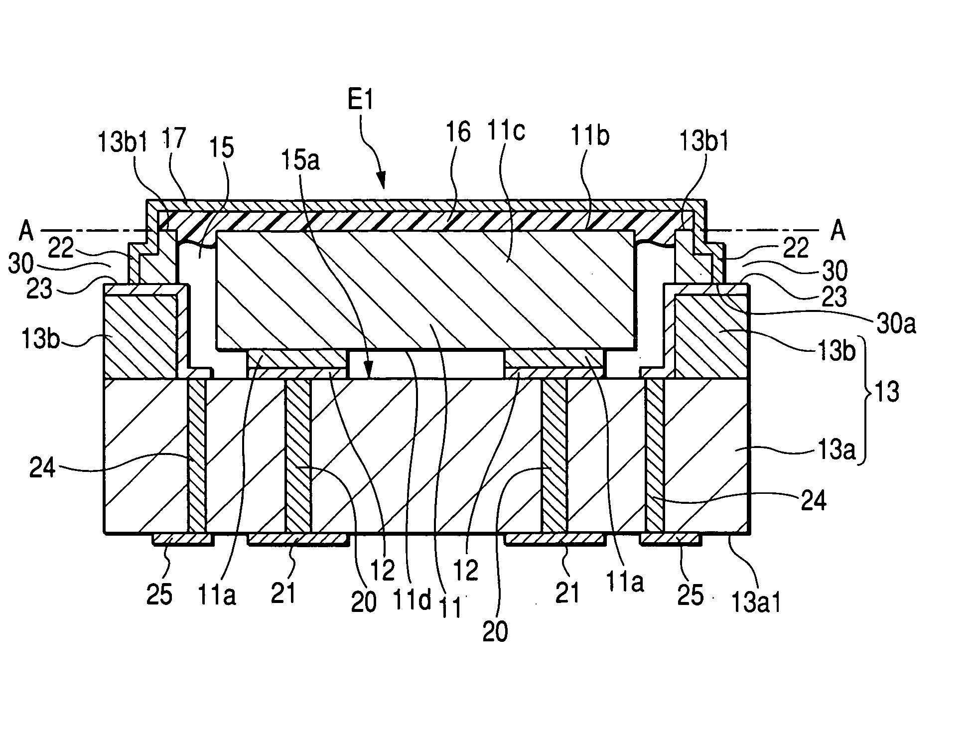
[0046]FIG. 1 is a cross sectional view of an electronic part according to the present invention. The electronic part shown in FIG. 1 is formed by sealing a surface acoustic element in a concave portion provided in a case body made of ceramic.

[0047] In the case body 13 composed of a laminated substrate made of ceramic in the electronic part E1 shown in FIG. 1, a concave portion is formed by providing a sidewall portion 13b on the bottom portion 13a. By this concave portion, an accommodating portion 15 for accommodating an electronic element 11 is formed. The substrate 11c of the electronic element 11 is accommodated in the accommodating portion 15 so that the surface 11d thereof is opposed to a bottom surface 15a of the accommodating portion 15, and thus the bottom surface 11b of the substrate 11c is directed upward.

[0048] The electronic element 11 is formed with terminals 11a, 11a, and the terminals 11a, 11a are electrically connected to connecting lands 12, 12 formed in the accomm...

second embodiment

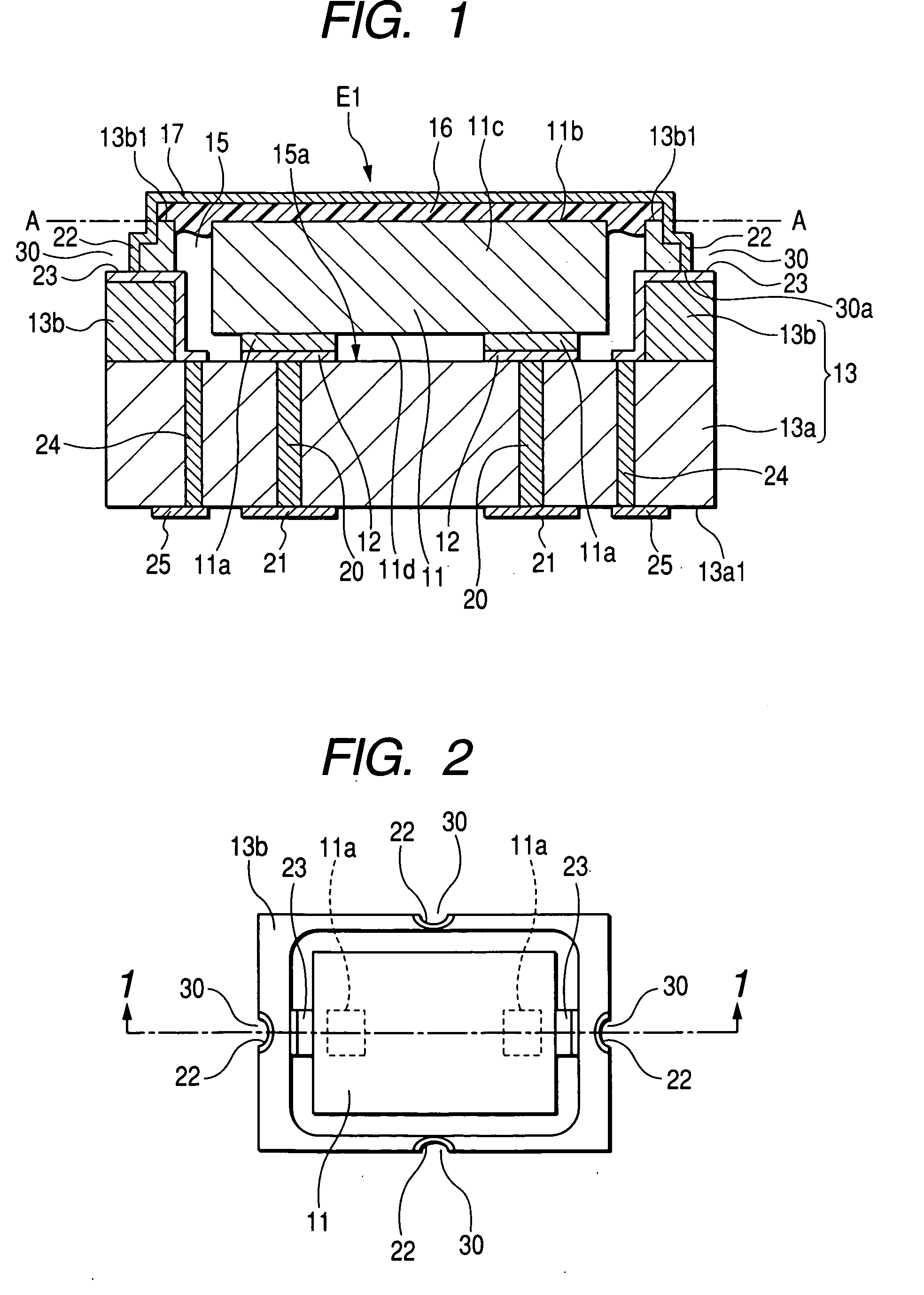
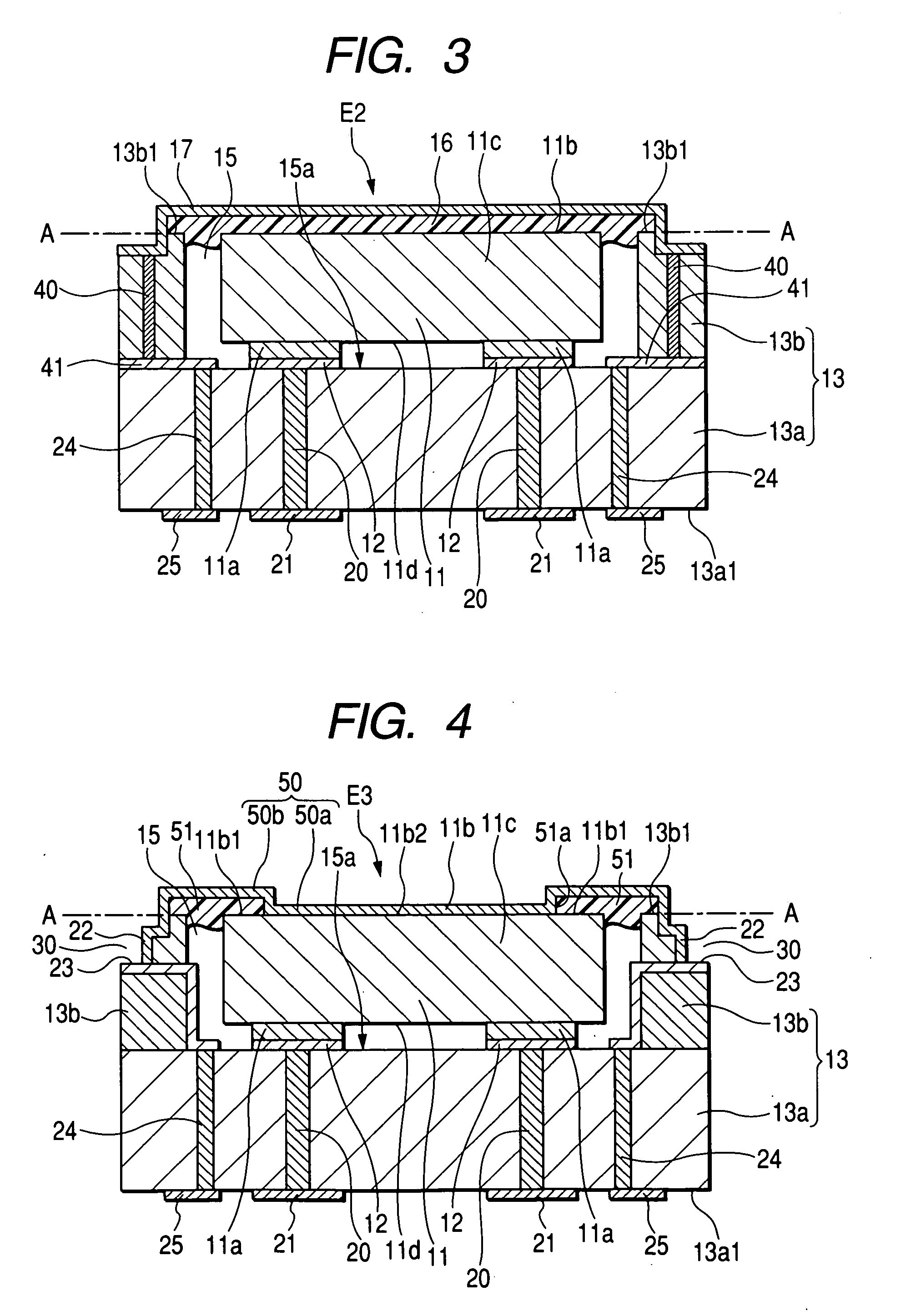
[0056] The plan view of the state that the metal film 17 of the electronic part of FIG. 1 is detached is shown in FIG. 2. Also, FIG. 1 is a cross sectional view when the electronic part cut along the line 1-1 in FIG. 2 is seen from the arrow direction. FIG. 3 is a cross sectional view of the electronic part E2 according to the present invention. The electronic part E2 shown in FIG. 3 is different from the electronic part E1 shown in FIG. 1 only in that a conductive portion 40 and a conductive portion 41 composed of conductive material are provided inside the sidewall portion 13b of the case body 13. The conductive portions 40, 41, 42 and the connecting portion 25 are electrically connected and the connecting portion 25 is grounded. By connecting the conductive portion 40 and the metal film 17, the metal film 17 is grounded and thus the shield effect of the metal film 17 can be improved.

[0057]FIGS. 4 and 5 are cross sectional views of electronic parts according to third and fourth em...


PUM


Abstract

An electronic part which can be miniaturized is provided. A bottom surface of a substrate of an electronic element is positioned on the same virtual plane of an upper surface of a sidewall portion of a case body, and a seal material is covered thereon. Accordingly, a gap between the seal material and the bottom surface of the electronic element is not formed, and thus the electronic part can easily be made thin. Also, since the seal material is formed by a resin, even when positions of the bottom surface of the substrate and an upper surface of the sidewall portion are deviated, the deviation can be easily absorbed.

Description

BACKGROUND OF THE INVENTION [0001] 1. Field of the Invention [0002] The present invention relates to an electronic part in which an electronic element is sealed in a case body and a method of manufacturing the same, and more particularly to an electronic part having a miniaturized case body and a method of manufacturing the same. [0003] 2. Description of the Related Art [0004]FIGS. 17 and 18 are cross sectional views showing the structure that a surface acoustic element is sealed in a concave portion provided in a case body made of ceramic. The structure of FIG. 17 is described in Japanese unexamined Patent Application Publication No. 2001-77659 and the structure of FIG. 18 is described in Japanese unexamined Patent Application Publication No. 2003-87093. [0005] A case body 3 of an electric part shown in FIG. 17 is formed with the concave portion, and an accommodating portion 5 in which an electronic element 1 is accommodated by the concave portion is formed. The electronic element ...

Claims


Application Information

Patent Timeline
Patent Type & Authority Applications(United States)
IPC IPC(8): H01L23/10H01L23/02H01L23/08H03H3/08H03H9/02
CPCH03H3/08H03H9/1085H03H9/1078H03H9/02913H01L2224/16225H01L2224/73253H01L2924/16152H01L2924/16195
Inventor TAKEUCHI, HIDEAKISASAKI, HITOSHIKONDO, HIDEKIWAGA, SATOSHI
Owner ALPS ALPINE CO LTD
Learn More