World line structure with single-sided partially recessed gate structure
- Summary
- Abstract
- Description
- Claims
- Application Information
AI Technical Summary
Benefits of technology
Problems solved by technology
Method used
Image
Examples
Embodiment Construction
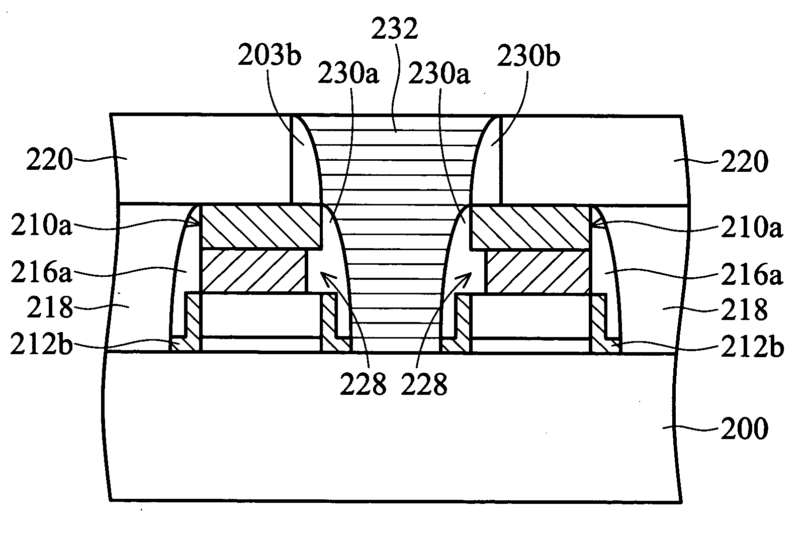
[0024]FIGS. 2a to 2g are cross-sections showing a method for forming a word line structure with a single-sided partially recessed gate structure for a semiconductor device, such as a DRAM.
[0025] First, in FIG. 2a, a substrate 200, such as a silicon substrate, is provided. The substrate 200 may contain semiconductor devices, such as capacitors and resistors, used in the memory devices. Here, in order to simplify the diagram, only a flat substrate is depicted. Next, a dielectric layer 202, a first conductive layer 204, a second conductive layer 206, and a capping layer (not shown) are successively formed overlying the substrate 200.
[0026] In the invention, the dielectric layer 202 is used for definition of a gate dielectric layer, which can be a silicon oxide layer formed by thermal oxidation. Moreover, the first conductive layer 204 is used for definition of a gate electrode, which can be a polysilicon layer. The second conductive layer 206 is used as a portion of the gate electrod...
PUM
 Abstract
Description
Claims
Application Information


