
Semiconductor device

A semiconductor, N-type semiconductor technology, applied in semiconductor devices, semiconductor/solid-state device manufacturing, transistors, etc., can solve the problems of semiconductor switch opening, voltage division, reaching or exceeding, etc., to achieve the effect of preventing opening

Active Publication Date: 2018-08-31
SHINDENGEN ELECTRIC MFG CO LTD
View PDF8 Cites 0 Cited by
  • Summary
  • Abstract
  • Description
  • Claims
  • Application Information

AI Technical Summary

Problems solved by technology

[0007] However, in the state where the reverse bias is applied, due to the high voltage applied between the first main electrode and the second main electrode, current leakage will occur in the first Zener diode and the second Zener diode connected in series. electric current
As a result, the high voltage applied between the first main electrode and the second main electrode will be divided due to this leakage current, causing the voltage of the control electrode to reach or exceed the turn-on threshold voltage inadvertently
As a result, it may cause the semiconductor switch to turn on

Method used


Image

  • Semiconductor device
  • Semiconductor device
  • Semiconductor device

Examples


no. 1 approach

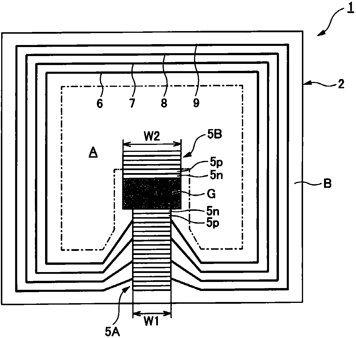
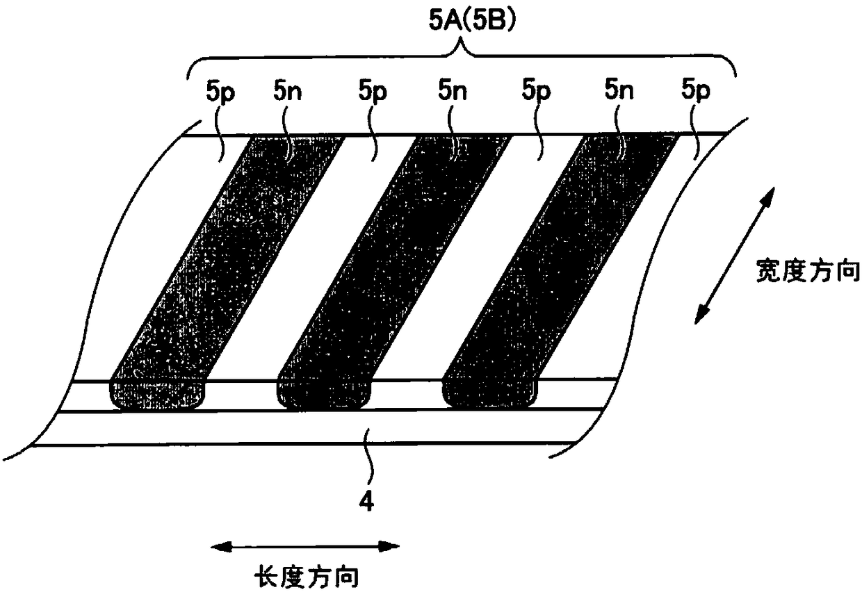
[0074] First, refer to Figure 1 ~ Figure 4 , the semiconductor device according to the first embodiment of the present invention will be described.

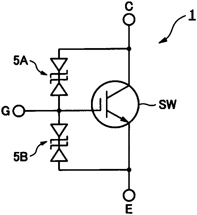
[0075] The semiconductor device 1 according to the first embodiment is, for example, figure 1 As shown, it includes: a semiconductor switch SW; a Zener diode 5A (first Zener diode); and a Zener diode 5B (second Zener diode).

[0076] The semiconductor switch SW has a first main electrode connected to a high potential, a second main electrode connected to a low potential, and a control electrode. The semiconductor switch SW has a MOS structure, and it is an insulated gate bipolar transistor (IGBT) in the present embodiment. The first main electrode is the collector electrode C, the second main electrode is the emitter electrode E, and the control electrode is the gate electrode G. The collector C is connected to a high potential (for example, 400V), and the emitter E is connected to a low potential (for example, ground). The ...

no. 2 approach

[0099] Next, we will refer to Figure 5 , the semiconductor device according to the second embodiment of the present invention will be described. In the second embodiment, the Zener diode 5B between the gate emitters is regarded as a bipolar transistor, and the leakage current between the gate emitters is increased by increasing the current amplification factor of the transistor to suppress the gate voltage. rise. Next, the second embodiment will be described focusing on points of difference from the first embodiment.

[0100] Like the semiconductor device 1 according to the first embodiment, the semiconductor device according to the second embodiment includes: a semiconductor switch SW; a Zener diode 5A; and a Zener diode 5B.

[0101] As described above, the concentration of the P-type dopant in the P-type semiconductor layer 5p constituting the Zener diodes 5A, 5B is lower than the concentration of the N-type dopant in the N-type semiconductor layer 5n. Therefore, if Fi...

no. 3 approach

[0108] Next, we will refer to Figure 6 ~ Figure 15 , the semiconductor device according to the third embodiment of the present invention will be described. In the third embodiment, by providing an integrated resistor connected in parallel with the Zener diode 5B, the leakage current between the gate and emitter electrodes is increased to suppress a rise in the gate voltage.

[0109] A semiconductor device 1A according to the third embodiment is, for example, Image 6 As shown, it includes: a semiconductor switch SW; a Zener diode 5A; a Zener diode 5B; and an integrated resistor R connected in parallel with the Zener diode 5B. The integrated resistor R is connected in parallel to the Zener diode 5B as described later, and is integrated (integrated) together with the Zener diode 5B. In other words, the integrated resistor R is not an external resistor.

[0110] In the present embodiment, among the plurality of N-type semiconductor layers 5n constituting the Zener diode 5B, t...


PUM

PropertyMeasurementUnit
Thicknessaaaaaaaaaa

Abstract

To prevent a semiconductor switch to be turned on in a reverse-bias-applied state. The invention comprises: a semiconductor switch SW provided with a collector electrode C, an emitter electrode E, anda gate electrode G; a zener diode 5A having one end electrically connected to the collector electrode C and the other end electrically connected to the gate electrode G, and configured in such a manner that an N-type semiconductor layer and a P-type semiconductor layer are disposed adjacent to one another; and a zener diode 5B having one end electrically connected to the gate electrode G and theother end electrically connected to the emitter electrode E, and configured in such a manner that an N-type semiconductor layer and a P-type semiconductor layer are disposed adjacent to one another. The zener diode 5A and the zener diode 5B are configured in such a manner that, in a reverse-bias-applied state, the voltage of the gate electrode G does not rise to the ON threshold voltage of the semiconductor switch SW.

Description

technical field [0001] The present invention relates to a semiconductor device, in particular to a semiconductor device with a semiconductor switch and a Zener diode. Background technique [0002] Conventionally, a semiconductor device having a semiconductor switch including a so-called MOS structure has been widely known. In such a semiconductor device, a Zener diode is provided for overvoltage protection. However, Zener diodes are generally configured as a structure in which an N-type semiconductor layer and a P-type semiconductor layer are arranged adjacent to each other. [0003] For example, when the semiconductor switch is an insulated gate bipolar transistor (Insulated Gate Bipolar Transistor: IGBT), a first Zener diode is provided between the collector and the gate electrode, and a second Zener diode is provided between the gate electrode and the emitter. Zener diode. The first Zener diode and the second Zener diode are connected in series. [0004] Prior art lit...

Claims


Application Information

Patent Timeline
IPC IPC(8): H01L27/04H01L21/822H01L21/8234H01L27/06H01L27/088H01L29/78
CPCH01L29/866H03K17/06H03K17/082H03K17/74H03K2017/066H01L29/0692H01L29/4238H01L29/7395H01L27/0255H01L29/0688H01L29/36H03K17/08116
Inventor 小谷凉平松原寿树石塚信隆三川雅人押野浩
Owner SHINDENGEN ELECTRIC MFG CO LTD
Learn More