Semiconductor device

a technology of semiconductor devices and semiconductors, applied in semiconductor devices, semiconductor/solid-state device details, electrical apparatus, etc., can solve the problems of complex prioritizing soldering parts, deteriorating device radiation characteristics, and cracks in the soldering portion, so as to reduce the deterioration of heat dissipation characteristics and efficient heat dissipation

Inactive Publication Date: 2005-08-04
DENSO CORP
View PDF24 Cites 26 Cited by
  • Summary
  • Abstract
  • Description
  • Claims
  • Application Information

AI Technical Summary

Benefits of technology

[0037] Therefore, a parallel arrangement of the radiating surface of the first metal body and the radiating surface of the second metal body can be secured while at the same time achieving the primary objective of suppressing deterioration of heat dissipation characteristics

Problems solved by technology

However, in the conventional semiconductor device, an increased heat flux in the semiconductor element causes an excessive high temperature, which causes cracks in the soldering portion.
The crack in the solder interrupts a heat dissipation pa

Method used


Image

  • Semiconductor device
  • Semiconductor device
  • Semiconductor device

Examples


modified embodiment

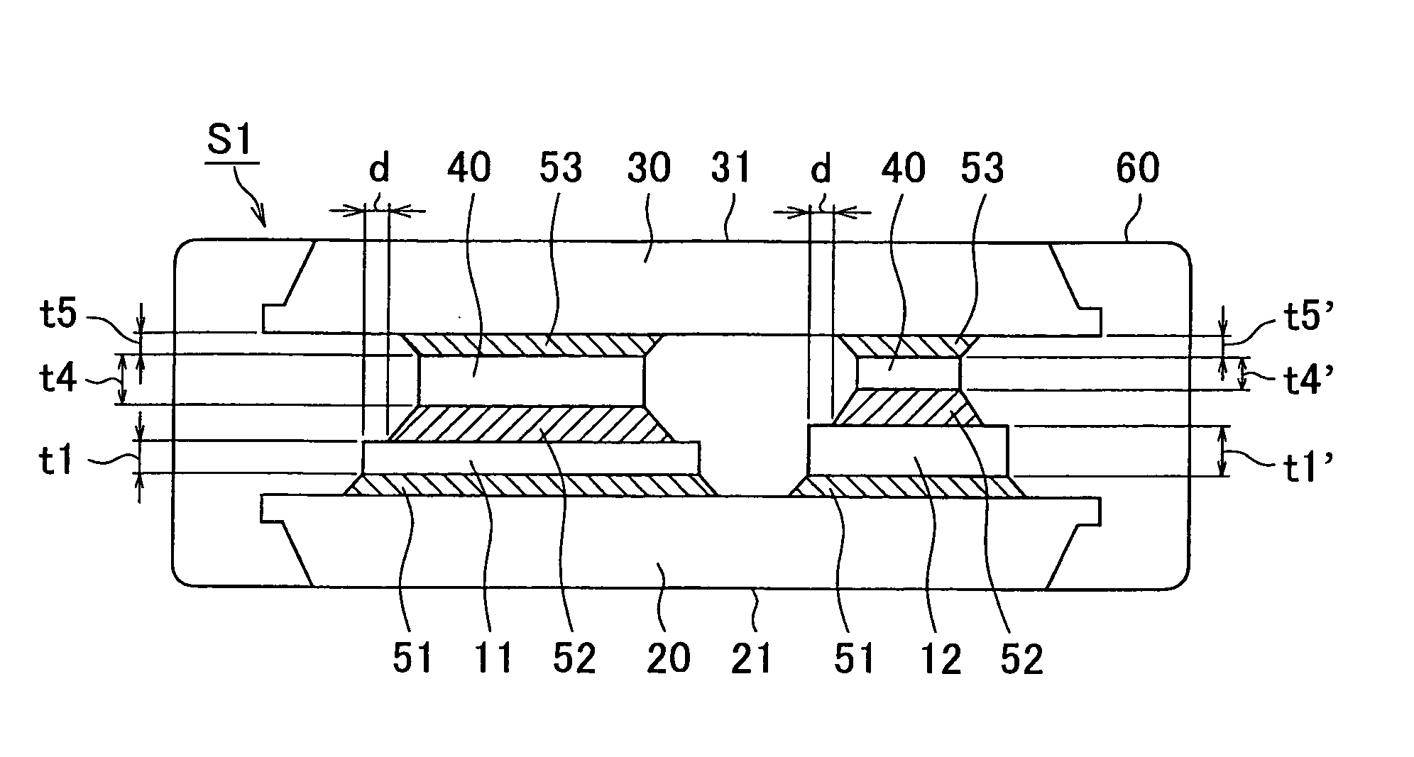
[0141] In the example shown in FIG. 1, the parallel arrangement of the radiating surfaces 21, 31 is achieved by changing the thickness t4, t4′ of each of the heat sink blocks 40, or the thickness t5, t5′ of each of the third solder portions 53 on each of the semiconductor chips 11, 12, when the thickness t1, t1′ of each of the plural semiconductor chips 11, 12 are different.

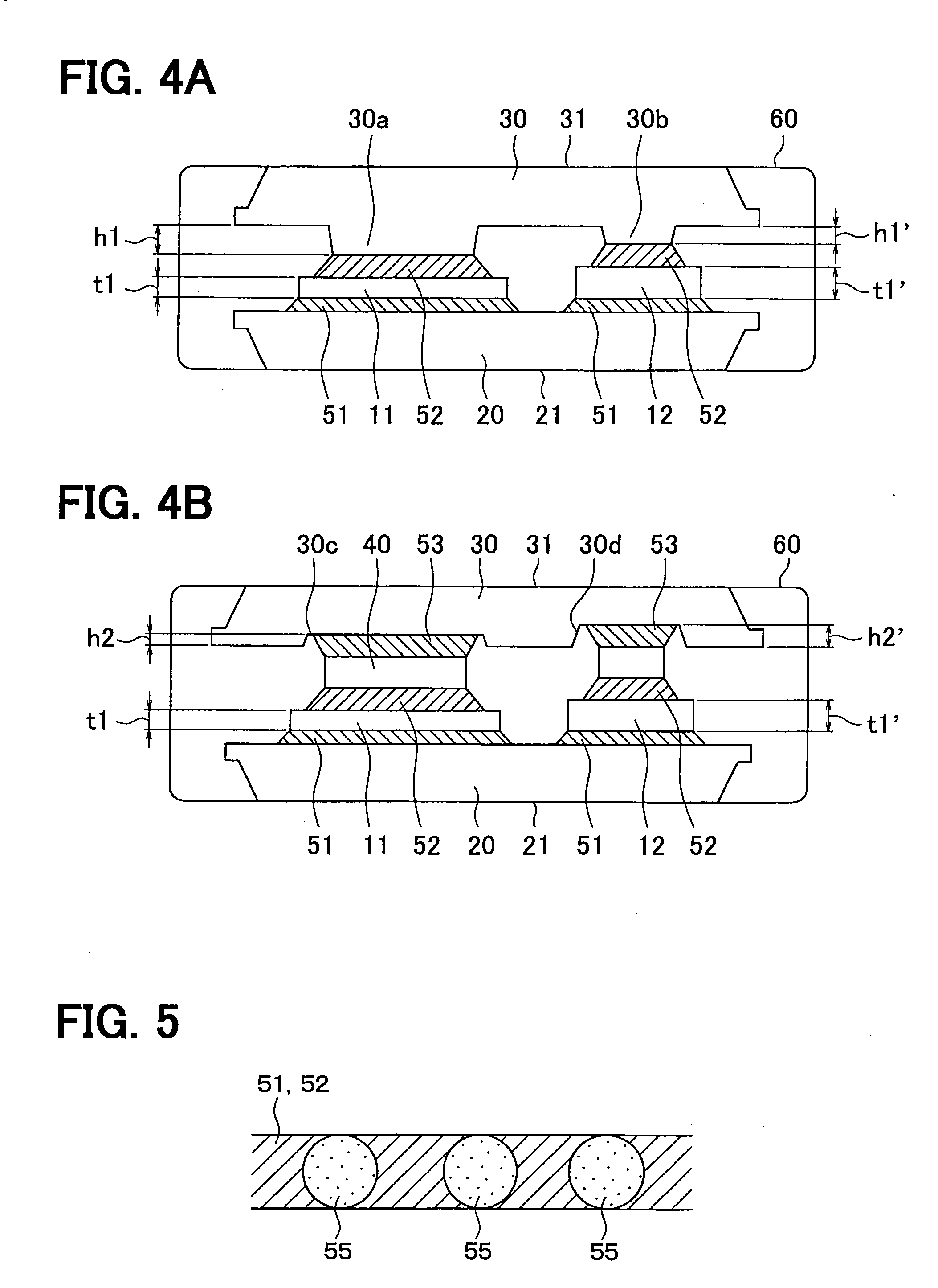
[0142] In this modified embodiment, a different method is devised to achieve the parallel arrangement. FIG. 4A and FIG. 4B show schematic cross sections of the first modified embodiment and the second modified embodiment respectively.

[0143] The semiconductor devices in FIG. 4A and FIG. 4B differ in the method to achieve the parallel arrangement of the radiating surfaces 21, 31, with the same structure in the remaining portion.

[0144] In the semiconductor devices in FIG. 4A and FIG. 4B, plural semiconductor chips 11, 12 of different thickness t1, t1′ are disposed on the same plane between the single lower heat s...


PUM


Abstract

A semiconductor device includes first and second semiconductor elements, a first metal body attached to a first side of the semiconductor elements by a first solder portion, a second metal body attached to a second side of the semiconductor elements with a second solder portion, and a resin mold sealing the semiconductor elements, the first metal body and the second metal body by encapsulating them. In the semiconductor device having the second side as an element disposition surface, strain measurement caused by heat stress is maximum at the first solder portion among soldering portions of the semiconductor elements.

Description

CROSS REFERENCE TO RELATED APPLICATIONS [0001] This application is based upon, claims the benefit of priority of, and incorporates by reference the contents of, Japanese Patent Application No. 2004-23000 filed on Jan. 30, 2004 and Japanese Patent Application No. 2004-291397 filed on Oct. 4, 2004. FIELD OF THE INVENTION [0002] The present invention relates generally to a semiconductor device molded with a resin and more particularly to a semiconductor device having metal bodies attached to opposite sides of a semiconductor element with a solder. BACKGROUND OF THE INVENTION [0003] A conventional semiconductor device generally includes a semiconductor element, a first electrode composed of a first metal body attached on a first side of the semiconductor element via a first solder, and a second electrode composed of a second metal body attached on a second side, which is opposite to the first side, via a second solder. The first and second electrodes have heat radiating properties. A re...

Claims


Application Information

Patent Timeline
IPC IPC(8): H01L23/40H01L21/28H01L21/44H01L21/50H01L21/60H01L23/02H01L23/34H01L23/433H01L23/488H01L23/492H01L25/07
CPCH01L23/4334H01L2224/32257H01L24/32H01L24/33H01L25/072H01L2224/32245H01L2924/01013H01L2924/01029H01L2924/01033H01L2924/0105H01L2924/01082H01L2924/13055H01L2924/01005H01L2924/01006H01L2924/01068H01L23/488H01L2224/32258H01L2924/1305H01L2924/1301H01L2924/3512H01L2924/00H01L2224/2612H01L2224/33181H01L2924/181H01L2924/351H01L2924/00012
Inventor HIRANO, NAOHIKOMAMITSU, KUNIAKI
Owner DENSO CORP
Why Eureka
Try Eureka