High-frequency power amplification electronic part and wireless communication system

a technology of power amplifier circuit and electronic part, applied in the direction of amplifier combination, automatic tone/bandwidth control, gain control, etc., can solve the problems of power inordinately reduced at lower temperatures, increased noise at higher temperatures, and increased gain at higher temperatures. achieve the effect of constant gain of the power amplifier circui

Active Publication Date: 2005-08-04
RENESAS ELECTRONICS CORP
View PDF9 Cites 68 Cited by
  • Summary
  • Abstract
  • Description
  • Claims
  • Application Information

AI Technical Summary

Benefits of technology

[0012] The above-outlined high-frequency power amplification electronic part of the invention generates bias currents or bias voltages each having a specific temperature characteristic, and supplies the generated currents or voltages to the multiple amplifier stages making up the power amplifier circuit in keeping with the characteristic of each of the power amplification transistors constituting the amplifier stages. The scheme makes it possible to keep the gain of the power amplifier circuit constant regardless of temperature variations.

Problems solved by technology

Where that control method is in use, noise can become greater at higher temperatures as the gain of the power amplifier circuit is varied with temperature.
If the gain of the power amplifier circuit is reduced so as to suppress noise, the gain can become too low—and power inordinately reduced—at lower temperatures.
However, the temperature compensation circuit utilizing the temperature-dependent diode characteristic has its own share of disadvantage: variations in detection output between diodes due to unsteady manufacturing procedures can cause the temperature compensation circuit to become unstable in controlling the gain.
This can make it difficult to achieve temperature compensation with stability and precision.

Method used


Image

  • High-frequency power amplification electronic part and wireless communication system
  • High-frequency power amplification electronic part and wireless communication system
  • High-frequency power amplification electronic part and wireless communication system

Examples


Embodiment Construction

[0025] Preferred embodiments of this invention will now be described with reference to the accompanying drawings.

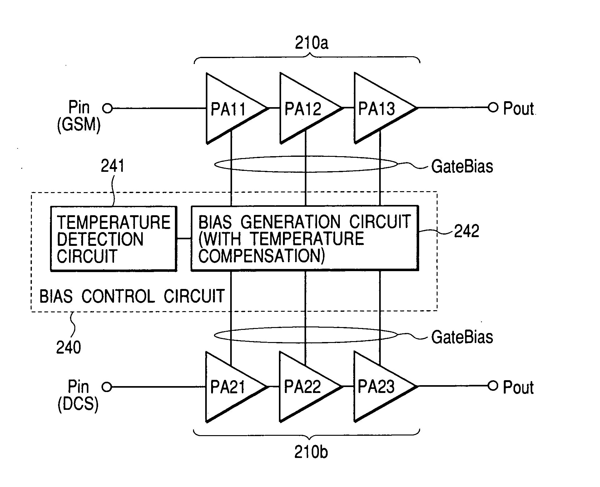
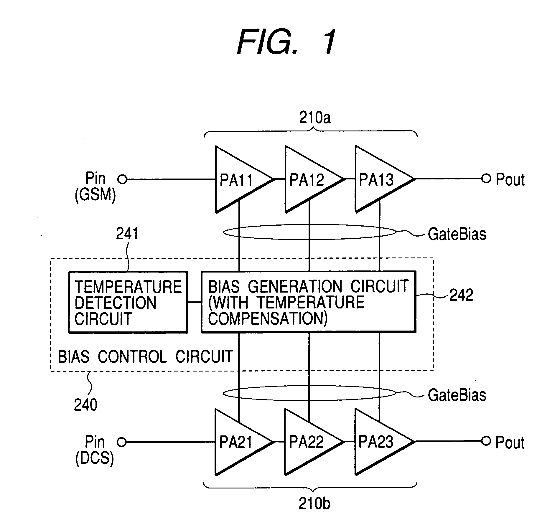
[0026]FIG. 1 is a block diagram outlining a typical structure of a high-frequency power amplifier block of a wireless communication system embodying the invention. This embodiment is structured as, but not limited to, a dual-band communication system using GSM and DCS. FIG. 1 shows two power amplifier circuits making up the system and a bias control circuit serving to bias these amplifier circuits.

[0027] In FIG. 1, reference numeral 210a stands for a power amplifier circuit that amplifies an outgoing signal at 900 MHz on the GSM frequency band; 210b denotes a power amplifier circuit that amplifies an outgoing signal at 1,800 MHz on the DSC frequency band; and 240 represents a bias control circuit that generates bias currents to be fed to the power amplifier circuits 210a and 210b.

[0028] The power amplifier circuits 210a and 210b are each constituted by three amplifier ...


PUM


Abstract

A high-frequency power amplification electronic part is disclosed which comprises a power amplifier circuit and a bias control circuit, the power amplifier circuit having a plurality of amplifier stages for amplifying an input high-frequency signal, the bias control circuit acting to bias the power amplifier circuit. The power amplifier circuit controls output power in accordance with input power that is varied while a gain of the power amplifier circuit is being fixed by either a bias current or a bias voltage supplied from the bias control circuit. The bias control circuit supplies at least two diode characteristic elements with a predetermined current each in order to generate at least two voltages demonstrating different temperature characteristics, the bias control circuit further using the generated voltages as a basis for generating either a plurality of bias currents or a plurality of bias voltages having a desired temperature-dependent rate of change each, the generated bias currents or bias voltages being fed to each of the plural amplifier stages constituting the power amplifier circuit.

Description

BACKGROUND OF THE INVENTION [0001] The present invention relates to a high-frequency power amplifier circuit which is used by a wireless communication system such as mobile telephones and which amplifies a high-frequency signal before outputting the amplified signal, and to an electronic part incorporating such a high-frequency power amplifier circuit. More particularly, the invention relates to a wireless communication system for varying input power of a high-frequency power amplifier circuit in order to control output power of the circuit, the output power being controlled while the gain of the high-frequency power amplifier circuit is being kept constant regardless of temperature variations. [0002] There has been in use a wireless communication system (mobile communication apparatus) such as a mobile telephone operating on a principle called GSM (Global System for Mobile Communication) that utilizes a frequency band of 880 through 915 MHz. GSM is based on a phase modulation metho...

Claims


Application Information

Patent Timeline
Patent Type & Authority Applications(United States)
IPC IPC(8): H03F3/68H03F1/30H03G3/30H04B1/04
CPCH03F1/301H03G3/3042H03F2200/372
Inventor NAGAMORI, HIROYUKITSUTSUI, TAKAYUKIMATSUSHITA, KOUICHI
Owner RENESAS ELECTRONICS CORP
Why Eureka
Try Eureka