ID label, ID tag, and ID card

a technology applied in the field of id labels and id tags, can solve the problems of reducing the lifetime affecting the life and reliability of id labels, and affecting the performance of id labels, so as to prevent the effect of idf chips, reduce the stress applied to thin film transistors, and thin thickness

Inactive Publication Date: 2005-08-04
SEMICON ENERGY LAB CO LTD
View PDF12 Cites 165 Cited by
  • Summary
  • Abstract
  • Description
  • Claims
  • Application Information

AI Technical Summary

Benefits of technology

[0008] Now, among commercial products and ID cards to which a non-contact type or contact type ID label or ID tag is attached, depending on the kinds, quite a lot of commercial products and ID cards are used in conditions with a wide range of temperature. In the case of attaching a non-contact type ID label or ID tag to that kind of commercial products, there is fear that, due to a difference between coefficients of thermal expansion of an antenna for communication and a resin provided around the antenna, stress is applied to the resin with the larger coefficient of thermal expansion to break the resin. In addition, in the case of attaching a contact type IC chip to the commercial products, there is fear again that, a resin is broken due to a difference between coefficients of thermal expansion of a contact electrode and the resin provided around the contact electrode. This naturally contributes to decrease in manufacturing yield, lifetime and reliability of an ID label or the like.
[0009] The present invention is made in view of the foregoing situation, and it is an object of the present invention to provide structures of an article such as an ID label, an ID tag, and an ID card and manufacturing processes thereof so that a resin covering an antenna or a contact electrode can be prevented from being broken due to stress even when an extreme difference in temperature is given to the ID label, the ID tag, and the ID card.

Problems solved by technology

In the case of attaching a non-contact type ID label or ID tag to that kind of commercial products, there is fear that, due to a difference between coefficients of thermal expansion of an antenna for communication and a resin provided around the antenna, stress is applied to the resin with the larger coefficient of thermal expansion to break the resin.
In addition, in the case of attaching a contact type IC chip to the commercial products, there is fear again that, a resin is broken due to a difference between coefficients of thermal expansion of a contact electrode and the resin provided around the contact electrode.
This naturally contributes to decrease in manufacturing yield, lifetime and reliability of an ID label or the like.

Method used


Image

  • ID label, ID tag, and ID card
  • ID label, ID tag, and ID card
  • ID label, ID tag, and ID card

Examples


embodiment mode 1

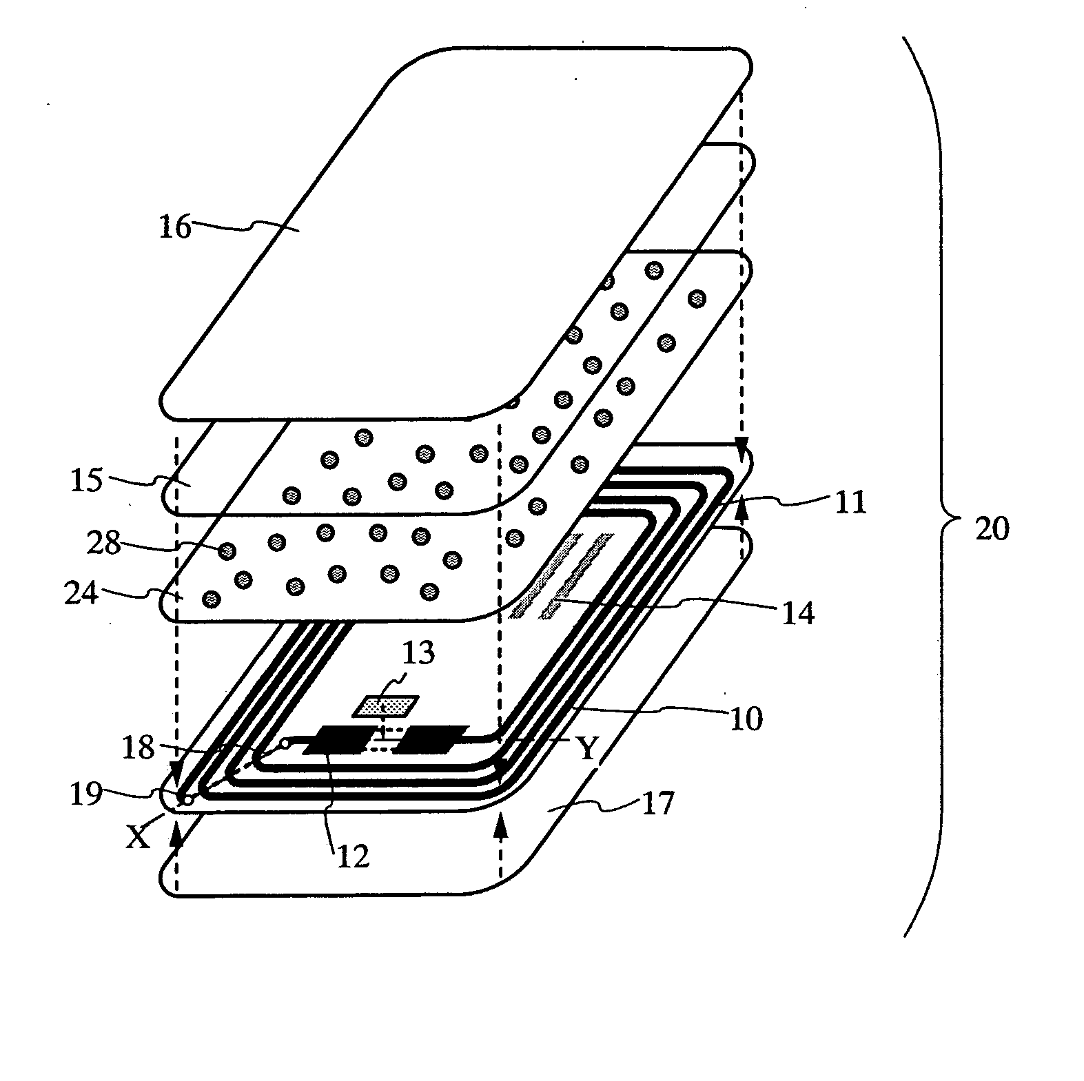
[0063] A structure and manufacturing method of an ID label according to the present invention will be described, mainly with reference to FIG. 1A, FIGS. 4A and 4B, and FIGS. 5A and 5B. FIG. 1A is a perspective view illustrating a structure of an ID label according to the present invention, where a substrate forming an ID label (generally referred to as “Tack Paper”, but not limited to paper) portion to be attached to a commercial product or the like is shown below and a separator to serve as a board of the label is show above for the sake of convenience.

[0064]FIG. 1A shows a case, where an antenna 11 and a connecting pad 12 that is a connecting portion connecting the antenna and a thin film integrated circuit device are formed in advance on a substrate 10 forming the ID label (hereinafter, which may be referred to as simply “a substrate” or “a label substrate”), and then, a thin film integrated circuit device 13 formed separately is attached to the label substrate. On a surface (a ...

embodiment mode 2

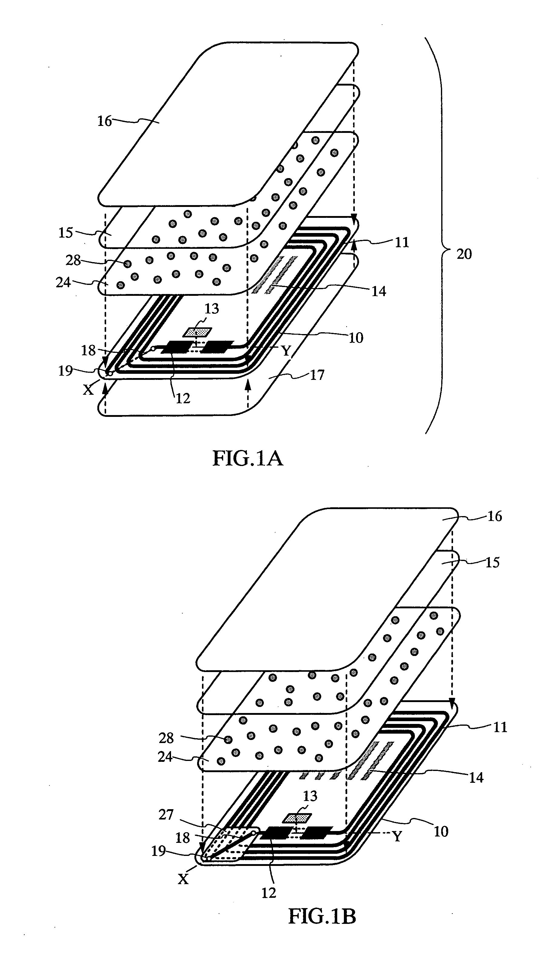
[0089] A structure and manufacturing method of an ID label according to the present invention will be described, mainly with reference to FIG. 1B and FIG. 6A. FIG. 1B is a perspective view illustrating a structure of an ID label according to the present invention, where a label substrate portion to be attached to a commercial product or the like is shown below and a separator to serve as a board of the label is show above for the sake of convenience.

[0090]FIG. 1B is the same as FIG. 1A in terms of showing a case, where an antenna 11 and a connecting pad 12 that is a connecting portion connecting the antenna and a thin film integrated circuit device are formed in advance on a label substrate 10, and then, a thin film integrated circuit device 13 formed separately is attached to the label substrate 10, and has a feature that a crossed wiring 18 connecting the thin film integrated circuit device 13 and the antenna 11 is formed on the inside of the label substrate 10.

[0091] In this ca...

embodiment mode 3

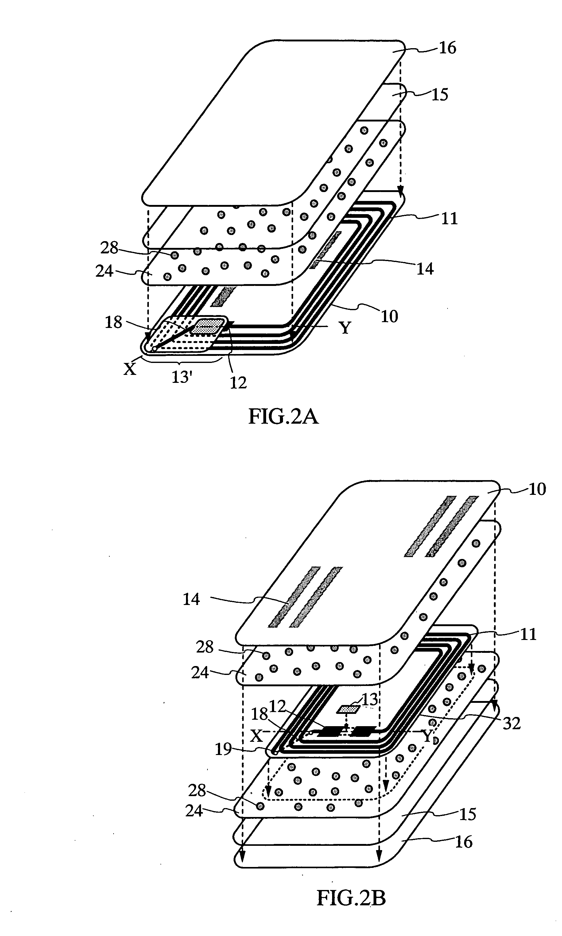
[0095] A structure and manufacturing method of an ID label according to the present invention will be described, mainly with reference to FIG. 2A and FIG. 6B. FIG. 2A is a perspective view illustrating a structure of an ID label according to the present invention, where a label substrate portion to be attached to a commercial product or the like is shown below and a separator to serve as a board of the label is show above for the sake of convenience.

[0096]FIG. 2A is the same as FIG. 1A in terms of showing a case, where an antenna 11 and a connecting pad 12 that is a connecting portion connecting the antenna and a thin film integrated circuit device are formed in advance on an ID label substrate 10, and then, a thin film integrated circuit device 13′ formed separately is attached to the substrate 10, and has a feature that a crossed wiring 18 connecting the thin film integrated circuit device 13′ and the antenna 11 is formed in the thin film integrated circuit device 13′.

[0097] The...


PUM


Abstract

In commercial products to which a non-contact type or contact type ID label or ID tag is attached and ID cards, there is fear that, due to a difference between coefficients of thermal expansion between an antenna for communication and a resin provided around the antenna, stress is applied to the resin with the larger coefficient of thermal expansion to break the resin. This contributes to decrease in manufacturing yield, lifetime, and reliability of an ID label or the like. In an article such as an ID label, an ID tag, and an ID card according to the present invention, a filler is included in a filling layer provided around an antenna forming an ID label, an ID tag, and an ID card so that the difference in coefficient of thermal expansion between the antenna and the filling layer can be reduced. This makes it possible to ease generation of stress due to the difference in coefficient of thermal expansion and prevent peeling and cracks of the filling layer.

Description

BACKGROUND OF THE INVENTION [0001] 1. Field of the Invention [0002] The present invention relates an article carrying a quite thin-model thin film integrated circuit that functions as a memory, a microprocessor (a central processing part, a CPU, or a MPU), or the like. The article includes, for example, an ID label, an ID tag, and an ID card, mainly for identifying human beings, animals and plants, commercial products, and the like. [0003] 2. Description of the Related Art [0004] Recently, in all kinds of industrial worlds such as food industry, manufacturing industry, or the like, calls have been heightened for strengthening safety and management systems of commercial products, and therewith, the amount of information on the commercial products are increasing. However, the current information on a commercial product is just information such as a country of manufacture, a manufacturer, an item number, or the like, mainly provided by ten and several figures of a bar cord, and the mou...

Claims


Application Information

Patent Timeline
Patent Type & Authority Applications(United States)
IPC IPC(8): G06K19/077G08B13/14
CPCG06K19/07722G08B13/2437G08B13/2417G06K19/07749G06K19/00G06K19/077
Inventor ARAI, YASUYUKIAKIBA, MAITACHIMURA, YUKOKANNO, YOHEI
Owner SEMICON ENERGY LAB CO LTD
Why Eureka
Try Eureka