

Flash memory cell, flash memory cell array and manufacturing method thereof
a flash memory cell and array technology, applied in the field of semiconductor devices, can solve the problems of difficult control of the amount of electrons flowing out of the floating gate, the size of the split-gate flash memory cell becomes larger than that of the conventional one, and achieve the effect of improving the programming speed and efficiency of the cell
- Summary
- Abstract
- Description
- Claims
- Application Information
AI Technical Summary
Benefits of technology
Problems solved by technology
Method used
Image

Examples
Embodiment Construction
[0034] Reference will now be made in detail to the present preferred embodiments of the invention, examples of which are illustrated in the accompanying drawings. Wherever possible, the same reference numbers are used in the drawings and the description to refer to the same or like parts.
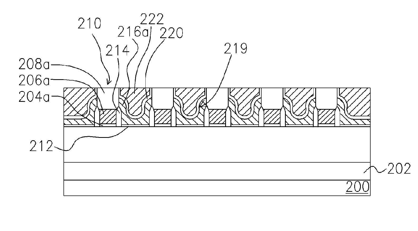
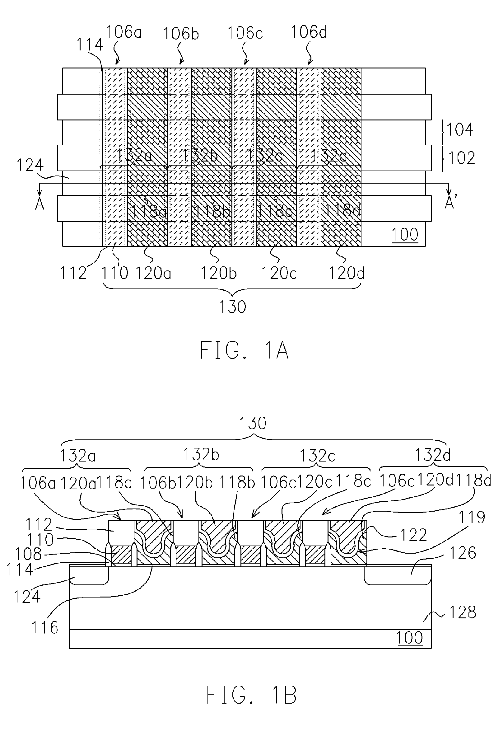
[0035]FIG. 1A shows a top view of a NAND type flash memory cell array of the present invention. FIG. 1B show the cross section (along A-A′ of FIG. 1A) of a NAND type flash memory cell array of the present invention.
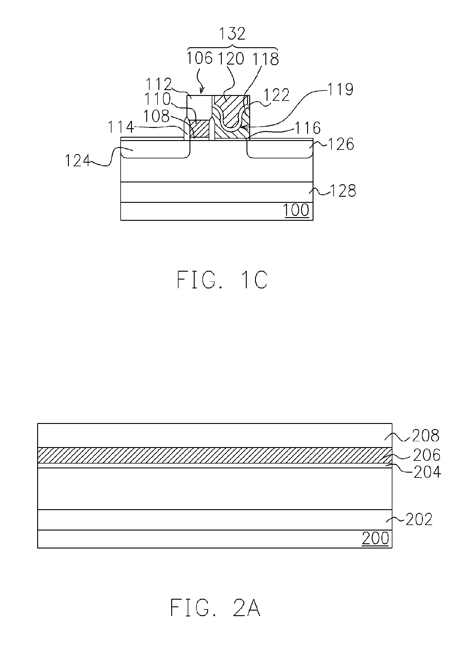
[0036] Referring to FIGS. 1A and 1B, the flash memory cell structure of the present invention comprise a substrate 100; a device insulating structure 102, an active region 104; a plurality of stack gate structures 106a-106d, wherein each of the stack gate structure includes a select gate dielectric layer 108, a select gate 110 and a gate cap layer 112); a spacer 114, a tunneling dielectric layer 116, a plurality of floating gates 118a-118d, a plurality of control gates 120a-120d, a plur...
PUM
 Abstract
Description
Claims
Application Information