Buried-contact solar cells with self-doping contacts

a solar cell and contact technology, applied in the field of photovoltaic solar cells, can solve the problems of high shadowing loss, time and cost of the process, relative complexity, etc., and achieve the effects of reducing the number of grid obscuration steps, and reducing the cost of production

Inactive Publication Date: 2005-08-11
APPLIED MATERIALS INC
View PDF99 Cites 131 Cited by
  • Summary
  • Abstract
  • Description
  • Claims
  • Application Information

AI Technical Summary

Benefits of technology

[0030] A primary advantage of the present invention is that it provides a less expensive solar cell with a minimum of grid obscuration.
[0031] Another advantage of the present invention is that it provides for elimination of numerous steps in the fabrication of a buried-contact solar cell, including elimination of heavy phosphorus diffusion steps and separate steps for electroless plating or other introduction of one or more metals to form the buried contact.

Problems solved by technology

The primary disadvantage of the prior art process sequence is the relative complexity, time, and expense of the process.
However, the self-doping metal contact methods have only been applied to surfaces, and suffer from high shadowing losses due to spreading out of the self-doping paste on the surface of the cell.

Method used


Image

  • Buried-contact solar cells with self-doping contacts
  • Buried-contact solar cells with self-doping contacts
  • Buried-contact solar cells with self-doping contacts

Examples


Embodiment Construction

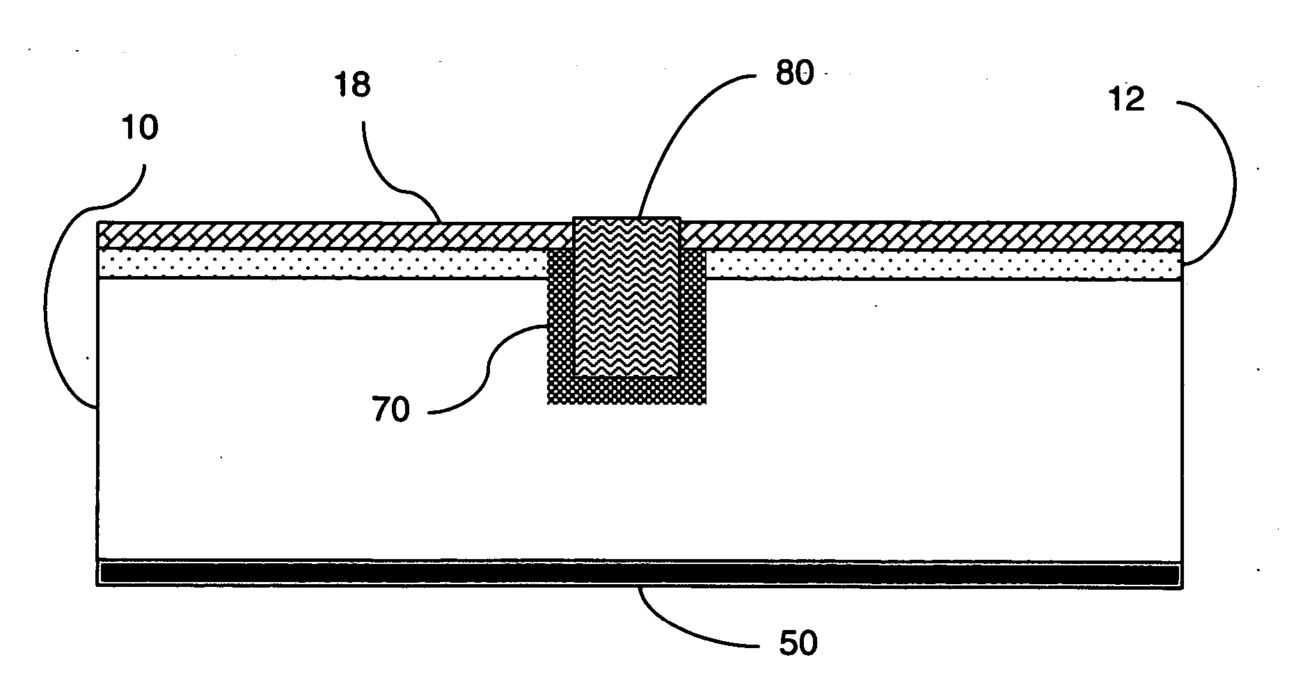
[0040] The present invention permits elimination of electroless plating sequences and provides for a simplified process for fabricating buried-contact solar cell structures, which buried-contact structures may be on either or both the front and back cell surfaces, by using a self-doping contact, including but not limited to a Ag:dopant paste.

[0041] A silicon substrate is typically multicrystalline or polycrystalline silicon, but other types of silicon substrates may be employed, including but not limited to single crystal, tricrystal, and thin crystalline-silicon films on glass or other substrates. Typically the silicon is a p-type semiconductor substrate. However, as described hereafter the invention may also be employed with n-type semiconductor substrates.

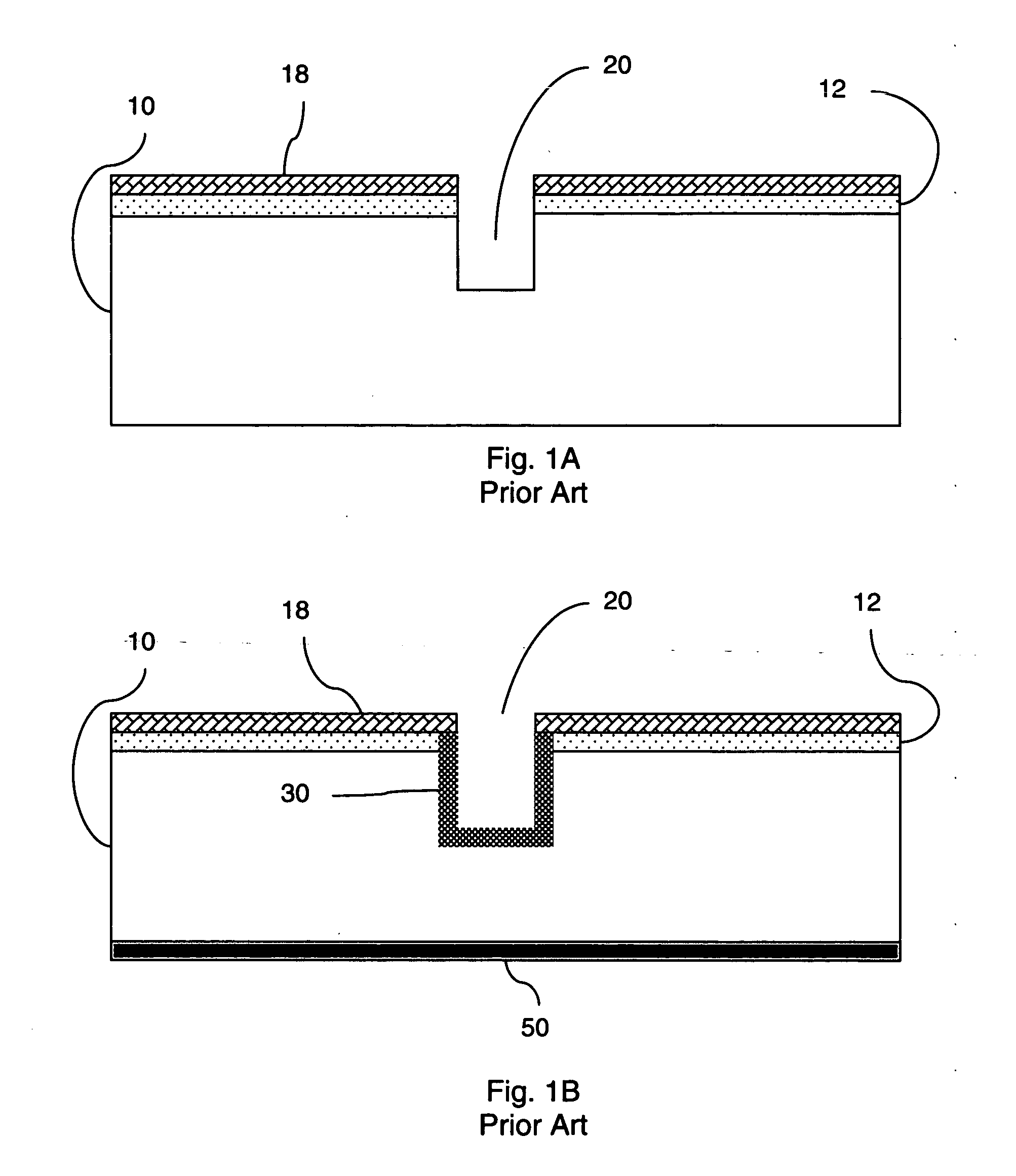
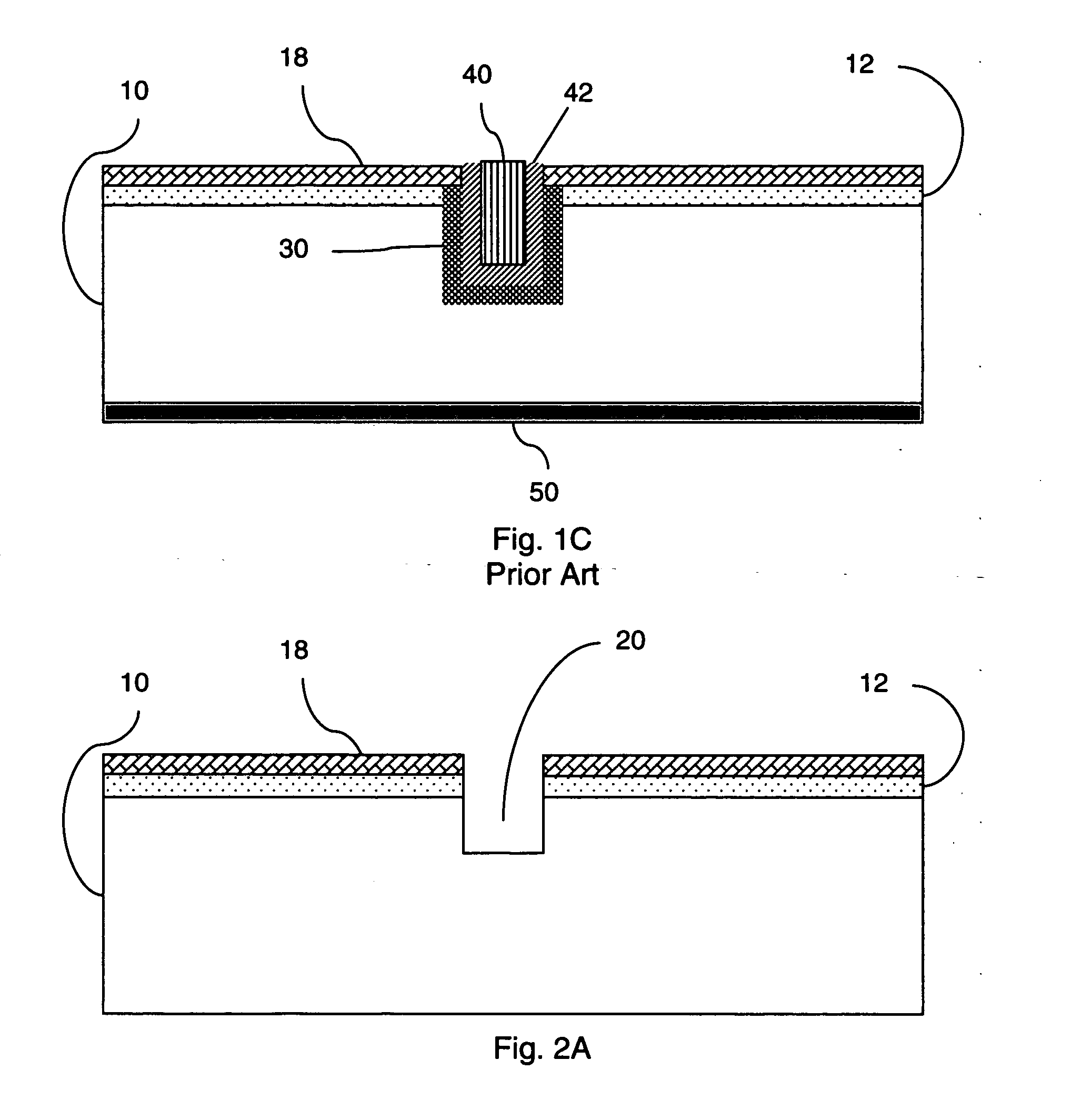
[0042] A preferred embodiment of the present invention provides a method for fabricating buried-contact cell structures that eliminates the heavy diffusion step and replaces the electroless plating sequence (two plating and on...


PUM


Abstract

A buried-contact solar cell, in-process buried-contact solar cell components and methods for making buried contact solar cells wherein a self-doping contact material is placed in a plurality of buried-contact surface grooves. By combining groove doping and metallization steps, the resulting solar cell is simpler and more economical to manufacture.

Description

CROSS-REFERENCE TO RELATED APPLICATIONS [0001] This application claims the benefit of the filing of U.S. Provisional Patent Application Ser. No. 60 / 542,454, entitled “Process for Fabrication of Buried-Contact Cells Using Self-Doping Contacts”, filed on Feb. 5, 2004, and of U.S. Provisional Patent Application Ser. No. 60 / 542,390, entitled “Fabrication of Back-Contact Silicon Solar Cells”, filed on Feb. 5, 2004. This application is related to U.S. Utility Patent Application Attorney Docket No. 31474-1005-UT, entitled “Contact Fabrication of Emitter Wrap-Through Back Contact Silicon Solar Cells”, by Peter Hacke and James M. Gee, filed concurrently herewith, and U.S. Utility Patent Application Attorney Docket No. 31474-1006-UT, entitled “Back-Contact Solar Cells and Methods for Fabrication”, by James M. Gee and Peter Hacke, also filed concurrently herewith. The specifications of all said applications are incorporated herein by reference.BACKGROUND OF THE INVENTION [0002] 1. Field of the...

Claims


Application Information

Patent Timeline
Patent Type & Authority Applications(United States)
IPC IPC(8): H01L21/00H01L21/8242H01L31/00H01L31/068
CPCH01L31/022425Y02E10/547H01L31/1804H01L31/068Y02P70/50H01L31/04H01L31/18
Inventor GEE, JAMES M.HACKE, PETER
Owner APPLIED MATERIALS INC
Why Eureka
Try Eureka