

Method and device for measuring wafer potential or temperature
a technology of potential or temperature measurement and measurement method, which is applied in the direction of fluid pressure measurement, semiconductor/solid-state device testing/measurement, instruments, etc., can solve the problems of difficult to measure the potential deterioration of the characteristics of the wafer b>, and achieve the effect of high reproducibility and mode of control of the wafer temperatur
- Summary
- Abstract
- Description
- Claims
- Application Information
AI Technical Summary
Benefits of technology
Problems solved by technology
Method used
Image

Examples
first embodiment
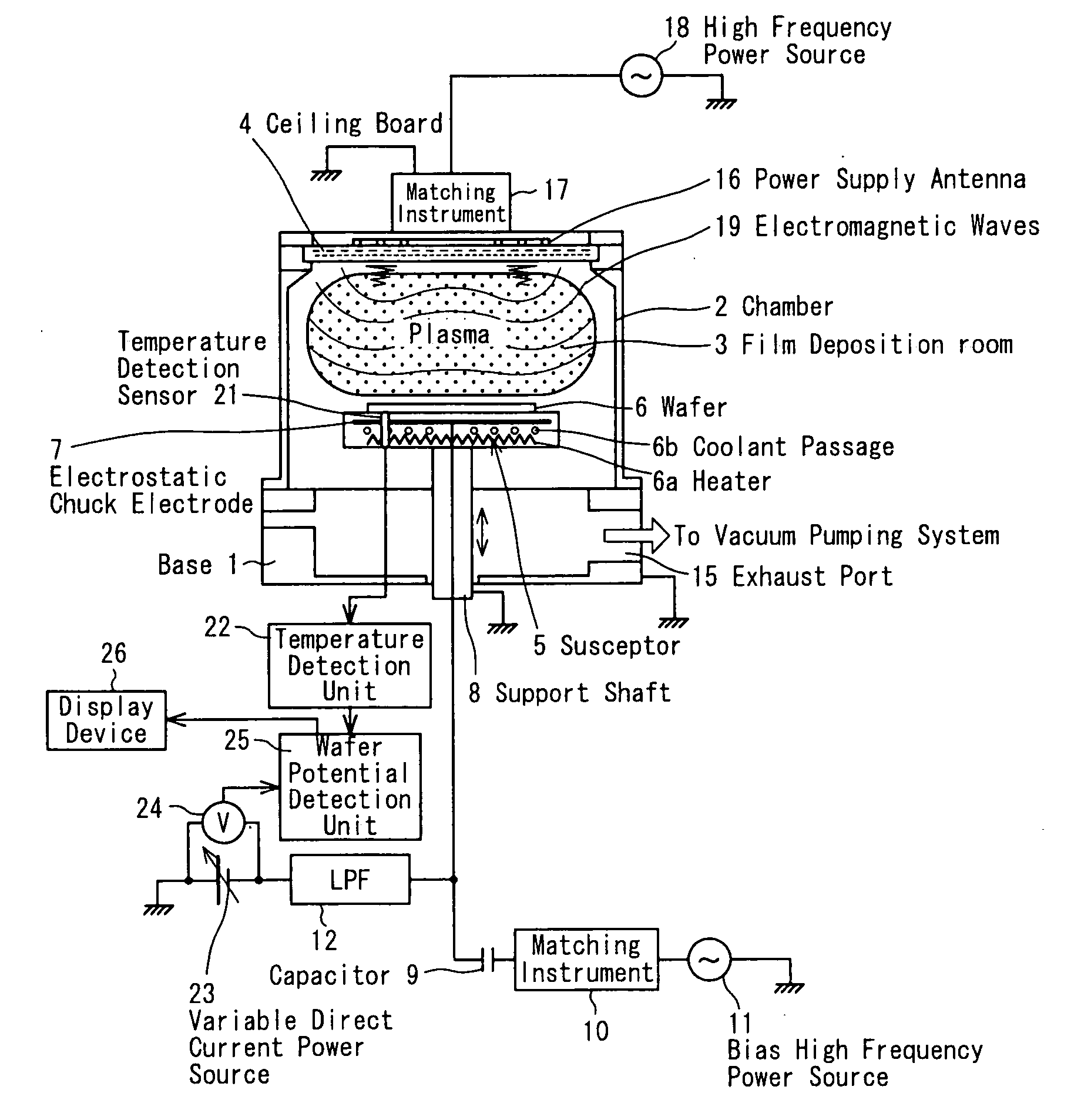
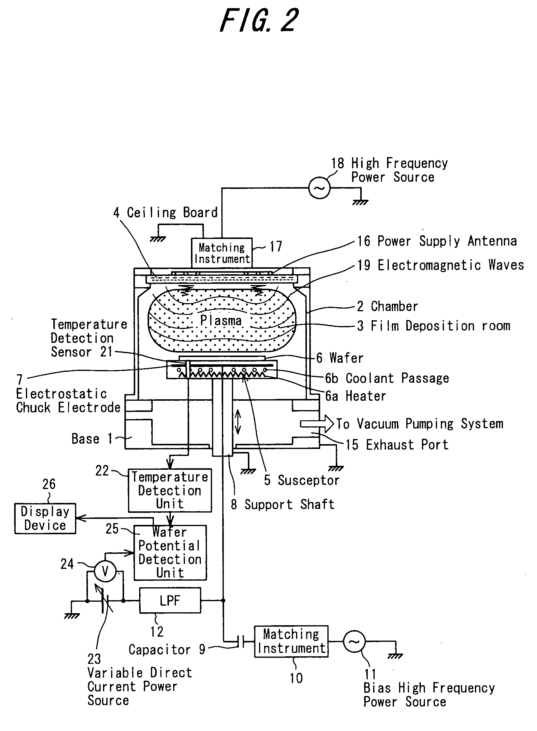
[0077]FIG. 2 is a configurational drawing showing a plasma CVD system incorporating a wafer potential measuring apparatus according to the first embodiment of the present invention. The plasma CVD system shown in the drawing is not essentially different from the plasma CVD system shown in FIG. 7, except that the wafer potential measuring apparatus is incorporated. In FIG. 2, therefore, the same portions as in FIG. 7 are assigned the same numerals, and duplicate explanations are omitted.
[0078] As shown in FIG. 2, the wafer potential measuring apparatus is composed of a temperature detection sensor 21, a temperature detection unit 22, a variable direct current power source 23, a voltmeter 24, a wafer potential detection unit 25, and a display device 26. The temperature detection sensor 21 can be preferably formed from an optical fiber piercing through the susceptor 5 in the following manner: A front end portion of the optical fiber is passed through the susceptor 5 to face the back o...
second embodiment
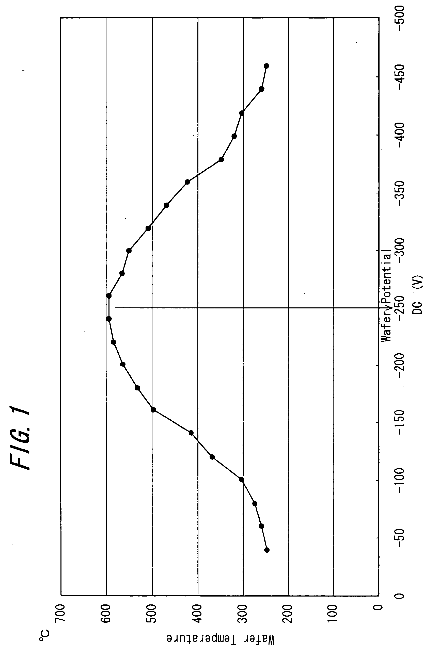
[0085]FIG. 4 is a configurational drawing showing a plasma CVD system incorporating a wafer temperature detecting apparatus according to an embodiment of the present invention. The plasma CVD system shown in the drawing is not essentially different from the plasma CVD system shown in FIG. 7, except that the wafer temperature detecting apparatus is incorporated. In FIG. 4, therefore, the same portions as in FIG. 7 are assigned the same numerals, and duplicate explanations are omitted.
[0086] As shown in FIG. 4, the wafer temperature detecting apparatus includes a temperature characteristic storage unit 31 for storing the temperature characteristics of the wafer 6, a variable direct current power source 32 capable of varying in output voltage, a voltage detector 33 for detecting the output voltage of the variable direct current power source 32, a display device 34 for displaying the temperature of the wafer 6, and a voltage control unit 35 for controlling the output voltage of the var...
PUM
| Property | Measurement | Unit |
|---|---|---|
| temperature | aaaaa | aaaaa |
| output voltage | aaaaa | aaaaa |
| temperature | aaaaa | aaaaa |
Abstract
Description
Claims
Application Information