
Eureka
For R&D, Eureka makes reading and utilizing patents & technical documents easy.
Eureka AIR
Designed for self-driven R&D workflows. Generate viable solutions, solve complex R&D challenges, empower your innovation with AI.

Eureka Materials
Designed for material experts only. Revolutionize your material R&D, from search, analyze, to developing new materials.

TechResearch
Generate reliable direction feasibility study reports for your R&D in just a few steps.

TechSeek
Discover and master advanced knowledge NOW. Basics, ideas, possibilities, all at once.

TechMind
As an expert in R&D Theories, TechMind can generates customized viable solutions instantly.

TechRisk
Analyze your overall solution with one click, know your potential R&D risks in advance.

TechMonitor
Get weekly tech updates, stay abreast of the latest tech innovations and key insights.
Method for forming metal oxide layer by nitric acid oxidation
- Summary
- Abstract
- Description
- Claims
- Application Information
AI Technical Summary
Benefits of technology
Problems solved by technology
Method used
Image

Examples
Embodiment Construction
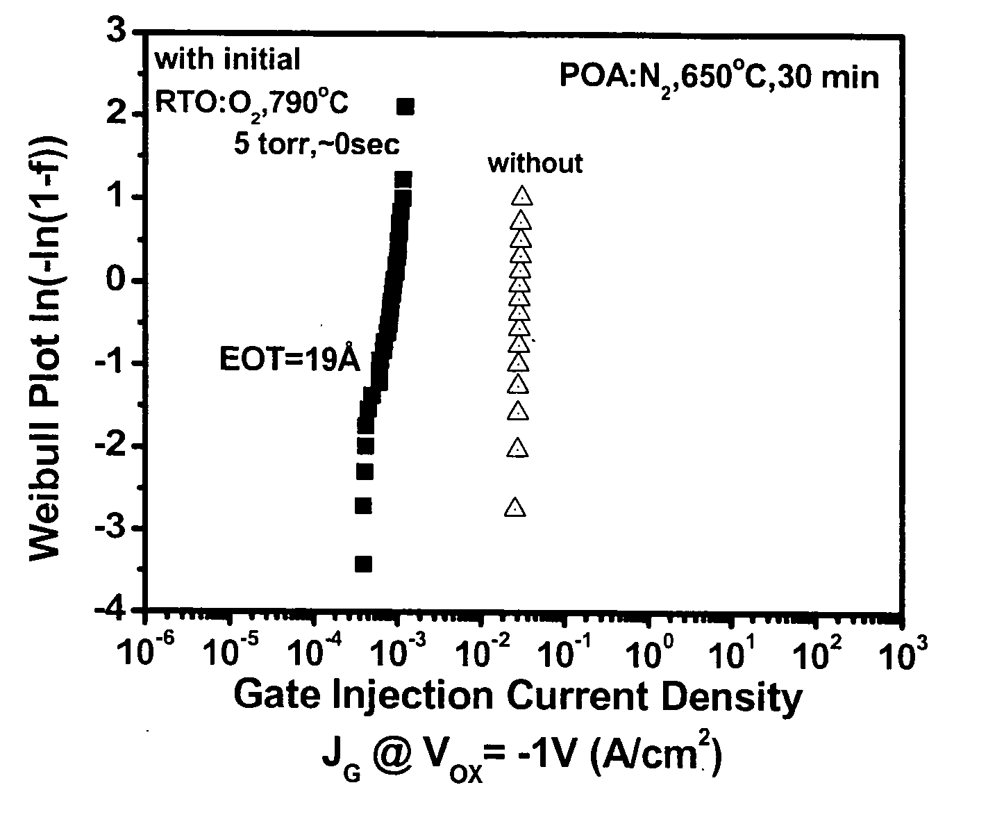
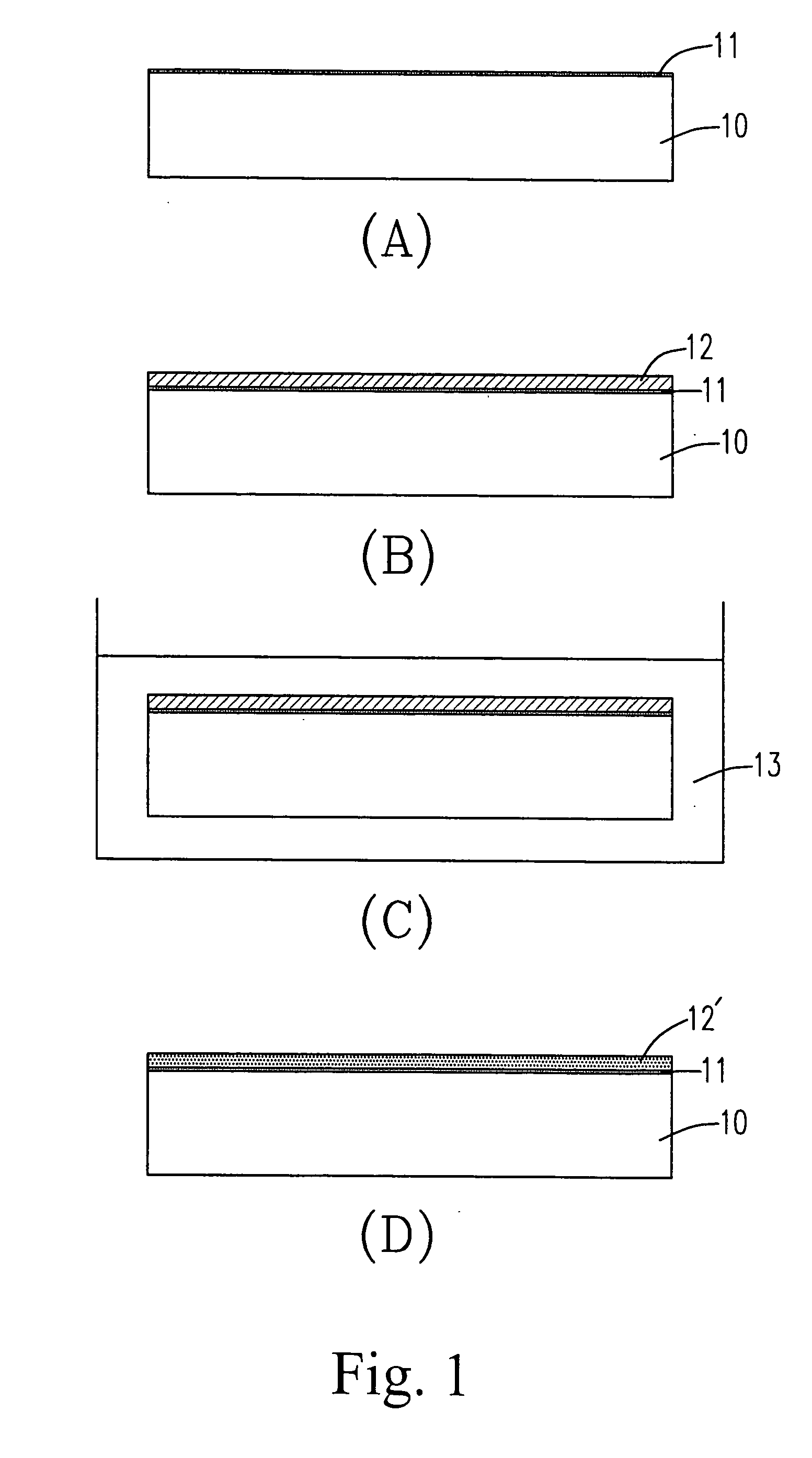
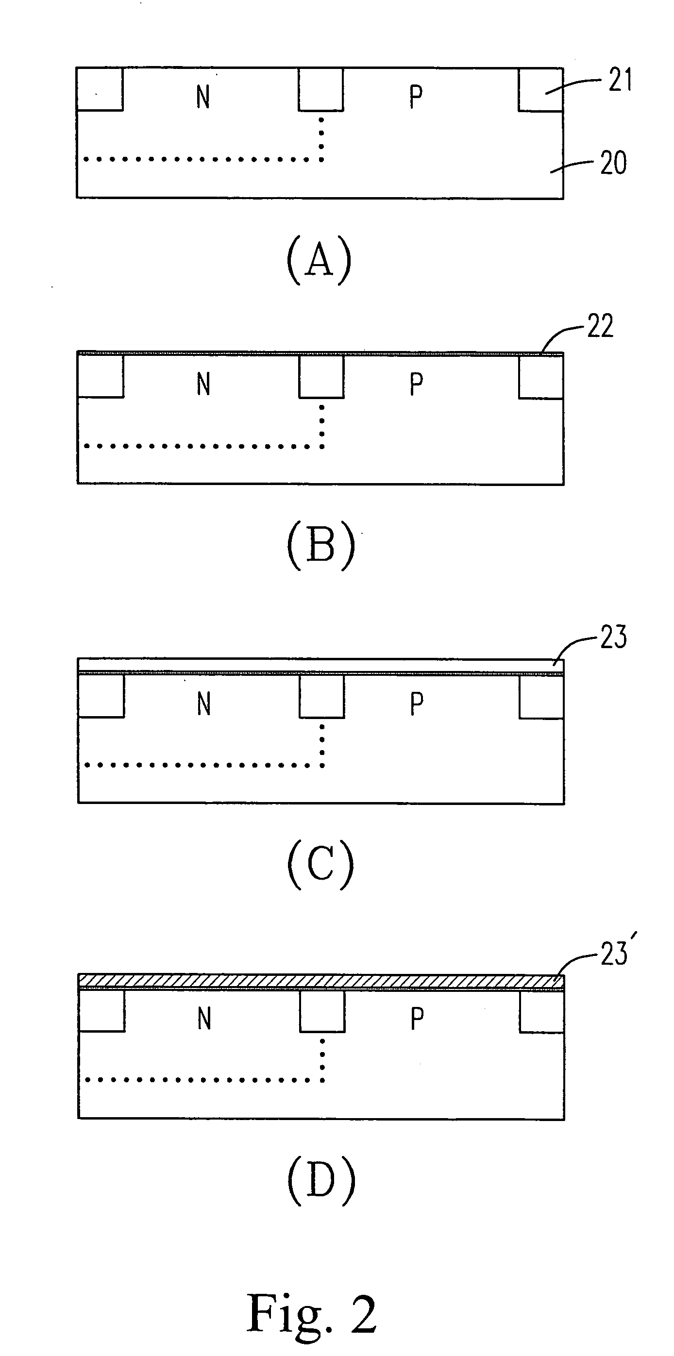
[0045] The present invention uses a high-k metal oxide layer to substitute the conventional silicon dioxide layer as the gate oxide layer, in which an ultra-thin silicon dioxide buffering interface is used to effectively avoid the generation of metal silicide between the high-k gate dielectric layer and the substrate. The manufacturing process of the present invention is to grow an ultra-thin silicon dioxide film on the semiconductor substrate as a buffering interface, and deposit an ultra-thin metal film, which is then oxidized into a metal oxide layer by a nitric acid oxidation and thermally annealed to increase the quality of the oxide layer. The method for forming the metal oxide layer of the present invention is illustrated in detail as follows.
[0046] Please refer to FIGS. 1(A) to (D) showing the method for forming the metal oxide layer according to a preferred embodiment of the present invention. First, a clean semiconductor substrate 10 is provided, in which the substrate ca...
PUM
 Abstract
Description
Claims
Application Information
 - R&D Engineer
- R&D Manager
- IP Professional
- Industry Leading Data Capabilities
- Powerful AI technology
- Patent DNA Extraction
Browse by: Latest US Patents, China's latest patents, Technical Efficacy Thesaurus, Application Domain, Technology Topic, Popular Technical Reports.
© 2024 PatSnap. All rights reserved.Legal|Privacy policy|Modern Slavery Act Transparency Statement|Sitemap|About US| Contact US: help@patsnap.com