
Eureka
For R&D, Eureka makes reading and utilizing patents & technical documents easy.
Eureka AIR
Designed for self-driven R&D workflows. Generate viable solutions, solve complex R&D challenges, empower your innovation with AI.

Eureka Materials
Designed for material experts only. Revolutionize your material R&D, from search, analyze, to developing new materials.

TechResearch
Generate reliable direction feasibility study reports for your R&D in just a few steps.

TechSeek
Discover and master advanced knowledge NOW. Basics, ideas, possibilities, all at once.

TechMind
As an expert in R&D Theories, TechMind can generates customized viable solutions instantly.

TechRisk
Analyze your overall solution with one click, know your potential R&D risks in advance.

TechMonitor
Get weekly tech updates, stay abreast of the latest tech innovations and key insights.
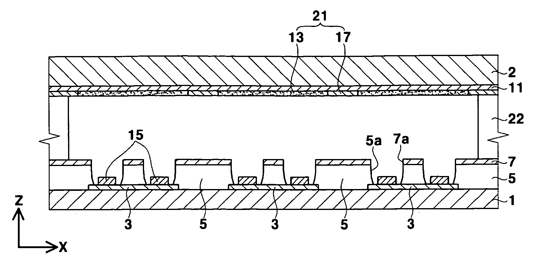
Method for forming electron emission source for electron emission device and electron emission device using the same
a technology of electron emission source and electron emission source, which is applied in the manufacture of electric discharge tube/lamp, tubes with screens, discharge tubes luminescnet screens, etc., can solve the problems of reducing the vacuum degree of vacuum device in vacuum device, shortened life of electron emission source, and surplus organic carbon that is mixed with carbon nanotubes that are not completely removed. , to achieve excellent life characteristics and electron emission characteristics
- Summary
- Abstract
- Description
- Claims
- Application Information
AI Technical Summary
Benefits of technology
Problems solved by technology
Method used
Image

Examples
example 1
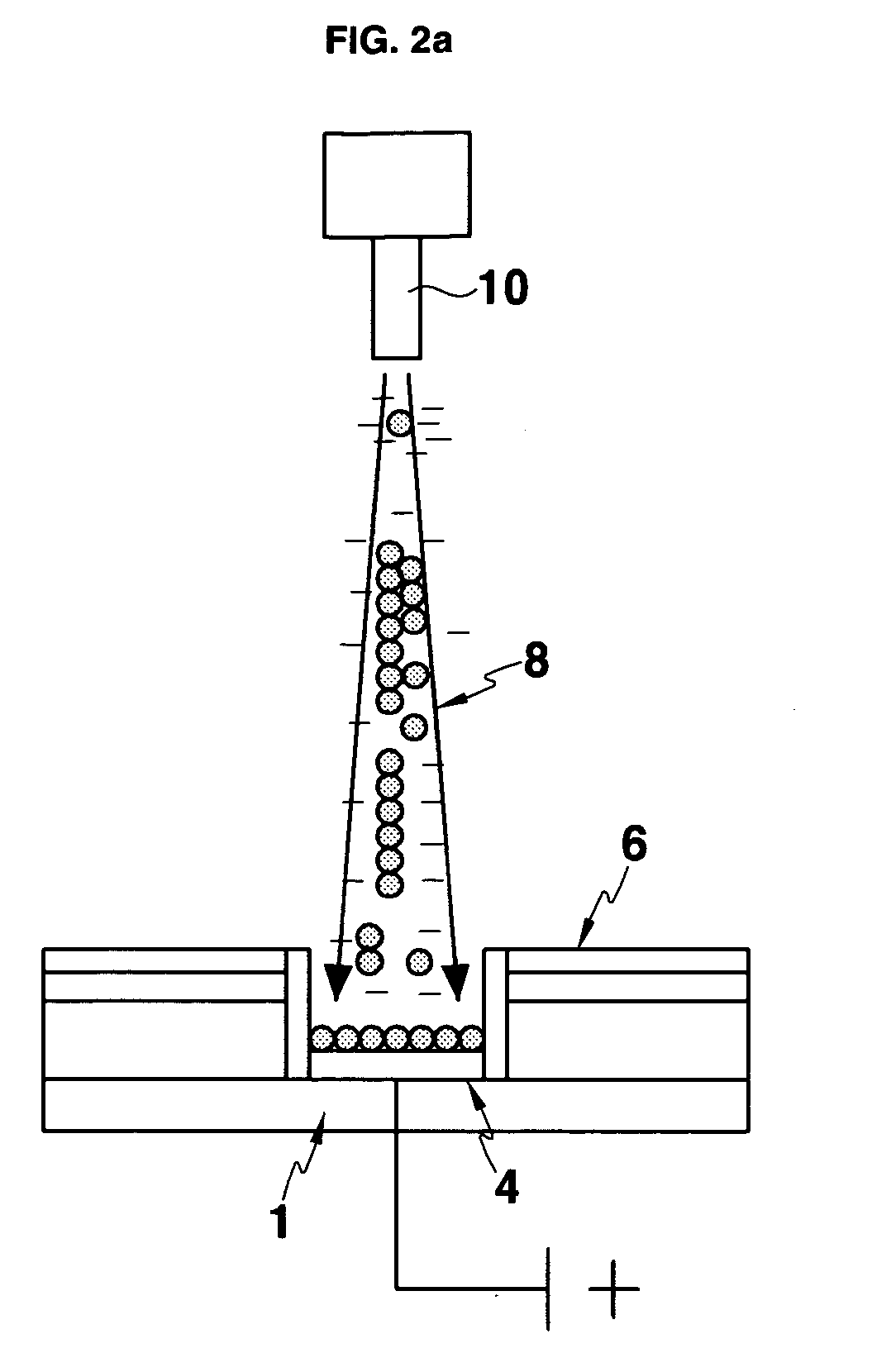
[0053] 10 g of the CNTs having 2-3 μm in diameter, 30 g of Ag as the metal particles having 1 μm in diameter, 20 g of the glass frit as the inorganic particles having 1 μm in diameter, and 40 g of a high molecular resin (isobutylmethacylate) were mixed to generate negative electric charges by using the electrostatic particle generator as shown in FIG. 2a according to the electrostatic coating principle. Then, the charged particles were uniformly sprayed on the positively charged substrate by a coating method. At this time, the substrate for the selective coating was patterned so that particles would only be deposited on selected portions by using the photoresist as the protection layer.
[0054] The metal particles were first deposited and then the CNT particles were deposited thereon. Then, the metal particles were deposited again more thinly and sparsely than the first time. Lastly, the CNTs were deposited by the same method. The CNTs remain as raised forms or well-defined forms on ...
experimental example
[0058] Concerning Example 1 and Comparative Example 1, the amount of electric current about the electron emission source was measured by a diode method. FIG. 4 shows a comparison of electron emission (I-V) characteristics of the electron emission source formed according to Example 1 of the present invention and the electron emission source of the conventional Comparative Example 1.
[0059] As shown in FIG. 4, the density of emitted electric current for the electron emission source formed through the coating by the electrostatic coating method of Example 1 of the present invention increased by more than 3 times at 5 V / um over a standard CNT electron emission source coated by the printing method using the conventional paste of Comparative Example 1. It is known that an operating voltage to obtain the same density of electric current (200 uA / cm2) can be also reduced more than 1 V / um. That is, the method of the present invention makes the formation of the CNT electron emission source wit...
PUM
 Abstract
Description
Claims
Application Information
 - R&D Engineer
- R&D Manager
- IP Professional
- Industry Leading Data Capabilities
- Powerful AI technology
- Patent DNA Extraction
Browse by: Latest US Patents, China's latest patents, Technical Efficacy Thesaurus, Application Domain, Technology Topic, Popular Technical Reports.
© 2024 PatSnap. All rights reserved.Legal|Privacy policy|Modern Slavery Act Transparency Statement|Sitemap|About US| Contact US: help@patsnap.com