Method and structure for CMOS device with stress relaxed by ion implantation of carbon or oxygen containing ions

a technology of cmos and ion implantation, which is applied in the direction of cmos or mosfet structure, semiconductor devices, electrical equipment, etc., can solve the problems of compressively stressed silicon, difficult to produce tensile-stressed silicon for n-fet areas, and complicated stressing of silicon in this manner, so as to prevent oxygen or carbon ion implantation, prevent the effect of implantation

Inactive Publication Date: 2005-08-25
TAIWAN SEMICON MFG CO LTD
View PDF77 Cites 52 Cited by
  • Summary
  • Abstract
  • Description
  • Claims
  • Application Information

AI Technical Summary

Benefits of technology

[0008] Preferred embodiments of the present invention include a CMOS structure having a stress-relaxed silicon nitride or SiN layer in which the stress is relaxed by the implantation therein of oxygen-containing or carbon-containing ions. The stress may be relaxed in selected areas of the SiN layer by preventing oxygen or carbon ion implantation in all but the selected areas, for example by appropriate masking. The stress may be tensile, as when the SiN layer is formed by TCVD, or compressive, as when the SiN layer is formed by PECVD. Typically, PMOS and NMOS devices will have been formed in and on the substrate following which these devices and the substrate will have been covered by the SiN layer. If the stress in the SiN layer is tensile, implantation of oxygen or carbon ions is prevented in areas of the layer overlying the NMOS devices. If the stress is compressive, the implantation is prevented in areas of the layer overlying the PMOS devices.

Problems solved by technology

Stressing silicon in this manner is somewhat complicated.
Moreover, it has been found difficult to produce tensile-stressed silicon for n-FET areas (to enhance electron mobility) and compressively stressed silicon for p-FET areas where both are present in a single structure, ibid.

Method used


Image

  • Method and structure for CMOS device with stress relaxed by ion implantation of carbon or oxygen containing ions
  • Method and structure for CMOS device with stress relaxed by ion implantation of carbon or oxygen containing ions

Examples


Embodiment Construction

[0013] The making and using of the presently preferred embodiments are discussed in detail below. It should be appreciated, however, that the present invention provides many applicable inventive concepts that can be embodied in a wide variety of specific contexts. The specific embodiments discussed are merely illustrative of specific ways to make and use the invention, and do not limit the scope of the invention.

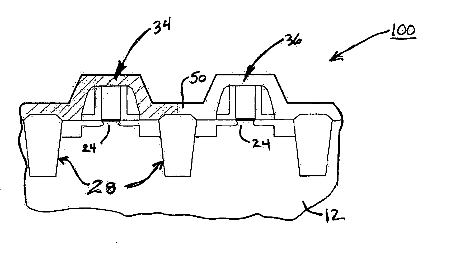
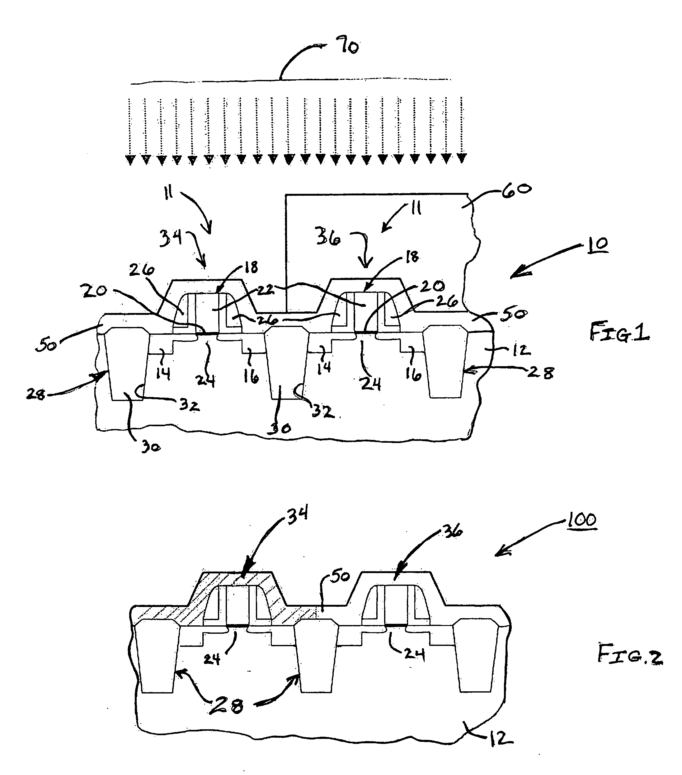
[0014] In FIG. 1 there is shown a prior art CMOS structure 10 that includes one or more transistors or other devices or elements, generally designated at 1. The structure 10, which is typically a small portion of an extensive integrated circuit or IC (not shown), includes a substrate 12. If the devices 11 are CMOS / MOSFET transistors, each may include an extended source 14 and an extended drain 16. Gate 18 resides between the source 14 and the drain 16.

[0015] As is conventional, the gate 18 includes a gate oxide or other dielectric 20, such as a high-K dielectric, that elec...


PUM

PropertyMeasurementUnit
thicknessaaaaaaaaaa
thicknessaaaaaaaaaa
stressaaaaaaaaaa

Abstract

Stress in a silicon nitride contact etch stop layer on a CMOS structure having NMOS and PMOS devices is selectively relieved by selective implantation of oxygen-containing or carbon-containing ions resulting in there being no tensile stress in areas of the layer above the PMOS devices and no compressive stress in areas of the layer above the NMOS devices.

Description

TECHNICAL FIELD [0001] The present invention relates to a CMOS structure that includes a silicon nitride layer, and, more generally, to a method of producing such a structure and its included silicon nitride layer. More specifically, the present invention relates to a CMOS or MOSFET structure that includes p-MOS (or p-FET) and n-MOS (or n-FET) areas over which a stressed, contact etch stop layer is formed, the stress in the layer being confined to those areas in which carrier mobility and drive current are enhanced thereby and avoided or eliminated in those areas in which carrier mobility and drive current are degraded thereby. BACKGROUND [0002] It is known that mechanical stress control in a channel region under a gate of a CMOS or MOSFET device can be crucial in the scaling down of device size. Mechanical stress—tensile and compressive—can increase the mobility of electrons and holes in the channel. In general, tensile stress improves electron mobility and degrades hole mobility, ...

Claims


Application Information

Patent Timeline
Patent Type & Authority Applications(United States)
IPC IPC(8): H01L21/4763H01L21/768H01L21/8238H01L29/76
CPCH01L21/31155H01L21/76825H01L21/76829H01L29/7843H01L21/823828H01L21/823871H01L29/7842H01L21/823807
Inventor CHENG, KUAN-LUNHUANG, HUAN-TSUNGCHENG, SHUI-MINGWANG, YIN-PINFUNG, KA-HING
Owner TAIWAN SEMICON MFG CO LTD
Why Eureka
Try Eureka