III-Nitride bidirectional switch

a bi-directional switch and nitride technology, applied in the field of semiconductor switches, can solve the problem of only blocking voltage in one direction, and achieve the effect of reducing costs

Active Publication Date: 2005-09-01
INFINEON TECH AMERICAS CORP
View PDF14 Cites 251 Cited by
  • Summary
  • Abstract
  • Description
  • Claims
  • Application Information

AI Technical Summary

Benefits of technology

[0008] A semiconductor switch according to the present invention is bidrectional and thus blocks voltage in both directions. This symmetry with respect to voltage blocking capability is achieved without sacrificing wafer material and, therefore, allows for cost reduction as well.
[0011] In another variation, a bidirectional switch according to the present invention includes two gate electrodes disposed between two ohmic electrodes. In this embodiment, each gate electrode is spaced from a respective ohmic electrode by the same distance. The use of two gate electrodes is advantageous in that it allows the voltage standoff region to be shared, thereby allowing for the reduction of the wafer area required for the transistor.

Problems solved by technology

However, these conventional devices block voltage only in one direction.

Method used


Image

  • III-Nitride bidirectional switch
  • III-Nitride bidirectional switch
  • III-Nitride bidirectional switch

Examples


first embodiment

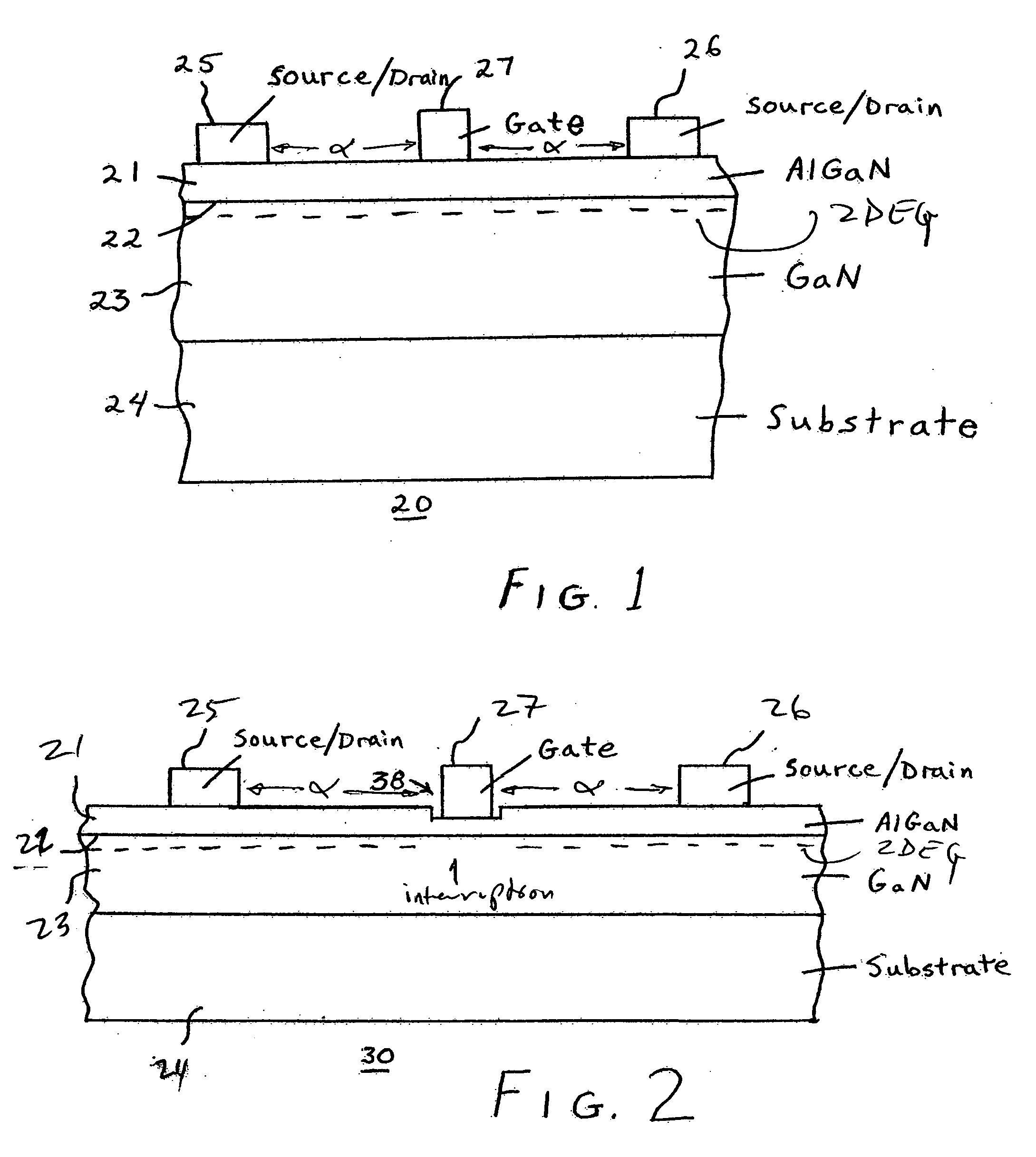
[0023] Referring now to FIG. 1, a bi-directional III-nitride switch according to the present invention is illustrated generally as a device structure 20. Device 20 includes substrate 24, which may be composed of Si, SiC, Sapphire, or the like, a first semiconductor body 23 formed over substrate 24 comprised of one III-nitride material, and a second semiconductor body 21 formed over first semiconductor body 23 and composed of another III-nitride semiconductor material having a band gap that is different from the one semiconductor material. It should be noted that first semiconductor body 23 need not be directly formed over substrate 24, but that a bottom layer may be interposed therebetween without deviating from the present invention. In the preferred embodiment, the one III-nitride semiconductor material is GaN and the another semiconductor material is AlGaN. As is known, the heterojunction 22 of GaN and AlGaN produces a highly conductive two-dimensional electron gas (2DEG) at or n...

third embodiment

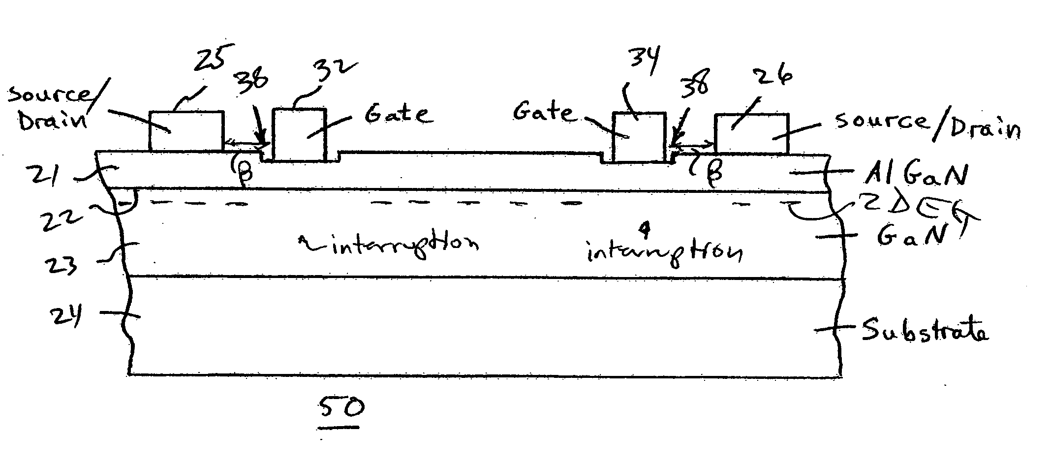
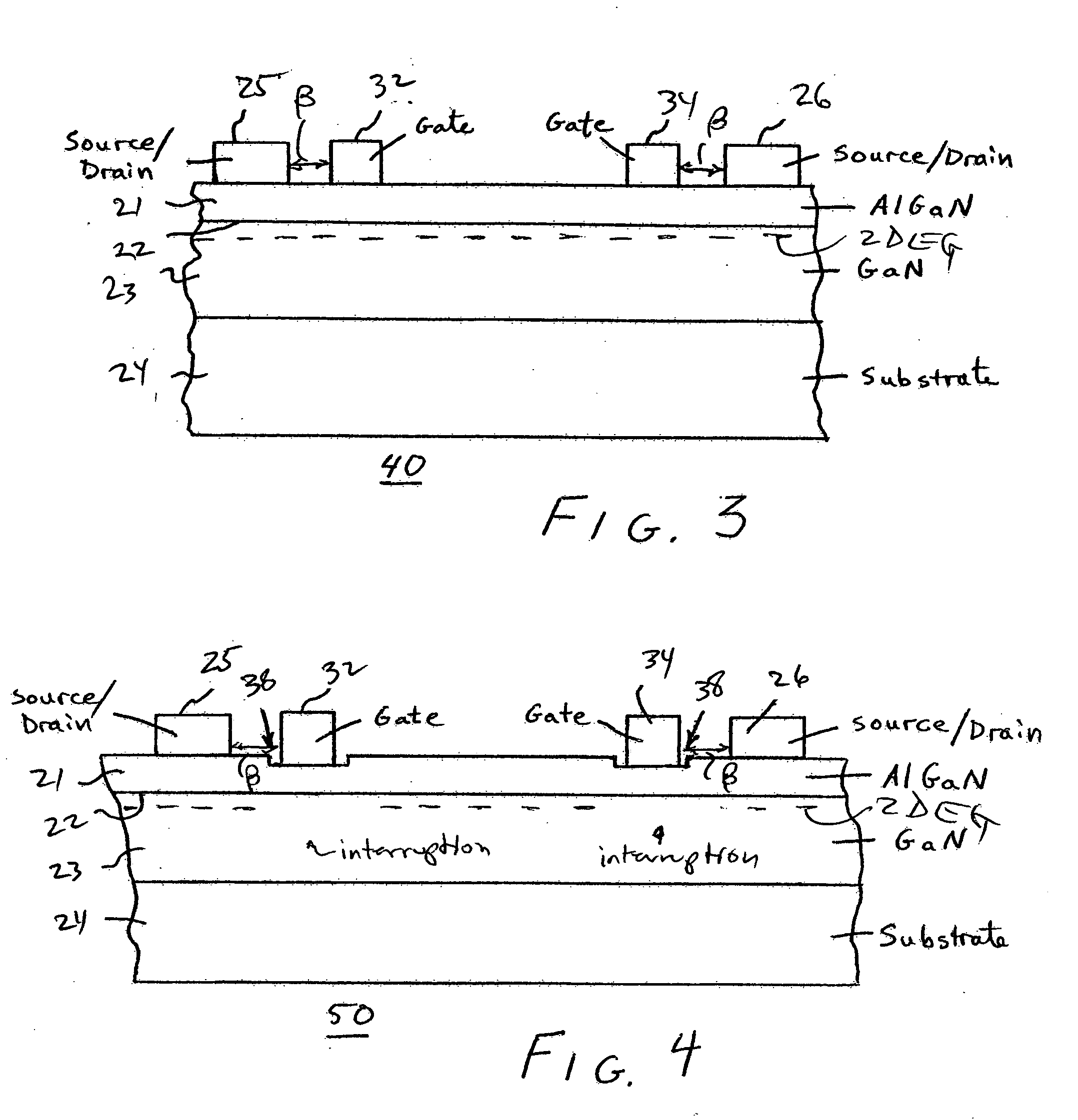
[0032] Referring now to FIG. 3, in which like numerals identify like features, device 40 according to the present invention includes two gate electrodes, first gate electrode 32 and second gate electrode 34. First gate electrode 32 is nearest to first ohmic electrode 25 and spaced from the same by a distance β. Second gate electrode 34 is nearest second ohmic electrode 26 and spaced from the same by a distance β as well. That is, first gate electrode 32 is spaced the same distance from first ohmic electrode 25 as second gate electrode 34 is from second ohmic electrode 26.

[0033] Device 40, according to the third embodiment is also a depletion mode device, meaning that it is nominally on. Specifically, the application of an appropriate voltage to either gate electrode 32, 34 causes an interruption in the 2DEG, whereby device 40 is turned off.

[0034] According to one aspect of the present invention, first gate electrode 32 and second gate electrode 34 are independently operable, meanin...

fourth embodiment

[0045] Referring next to FIG. 6, in which like numerals identify like features, a device according to either the third or the present invention includes two gate runners 46, 48. Each gate runner 46, 48 is electrically connected only to one of the gate electrodes 32, 34.

[0046] Referring to FIG. 7, in a device according to either the third or the fourth embodiment, each gate runner 46, 48 is electrically connected to a respective gate pad 50, 52, whereby each one of the gate electrodes 32, 34 becomes capable of independent operation. Also, it should be noted that all runners 40 connected to first ohmic electrode 25 are electrically connected to a respective common pad 54, and all runners 42 connected to second ohmic electrodes 26 are electrically connected to a respective common pad 56.

[0047] Referring now to FIG. 8, an alternate arrangement for gate electrodes and ohmic electrode 26, 25 is illustrated as structure 60. Structure 90 includes two gate electrodes, gate electrodes 32, 34...


PUM


Abstract

A III-nitride bidirectional switch which includes an AlGaN / GaN interface that obtains a high current currying channel. The bidirectional switch operates with at least one gate that prevents or permits the establishment of a two dimensional electron gas to form the current carrying channel for the bidirectional switch.

Description

CROSS-REFERENCE TO RELATED APPLICATION [0001] The present application is based on and claims benefit of U.S. Provisional Application No. 60 / 544,626 filed Feb. 12, 2004, entitled III-NITRIDE BIDIRECTIONAL SWITCH, to which a claim of priority is hereby made and the disclosure of which is hereby incorporated by this reference.BACKGROUND OF THE INVENTION [0002] 1. Field of the Invention [0003] The present invention relates generally to semiconductor switches, and relates more particularly to bidirectional semiconductor switches produced in a III-Nitride material system. [0004] 2. Description of Related Art [0005] Development of devices based on III-nitride materials has generally been aimed at high power-high frequency applications such as emitters for cell phone base stations. The devices fabricated for these types of applications are based on general device structures that exhibit high electron mobility and are referred to variously as heterojunction field effect transistors (HFETs), ...

Claims


Application Information

Patent Timeline
Patent Type & Authority Applications(United States)
IPC IPC(8): H01L31/0328
CPCH01L27/0605H01L29/7787H01L29/42316H01L29/2003H01L29/41758H01L29/66462H01L29/7783
Inventor KINZER, DANIEL M.BEACH, ROBERT
Owner INFINEON TECH AMERICAS CORP
Why Eureka
Try Eureka