
Display panel with signal transmission patterns

Inactive Publication Date: 2005-09-01
SAMSUNG ELECTRONICS CO LTD
View PDF5 Cites 15 Cited by
  • Summary
  • Abstract
  • Description
  • Claims
  • Application Information

AI Technical Summary

Benefits of technology

[0015] The present invention is to provide an integrated PCB that has a gate PCB and a data PCB on one board and is capable of allowing driving signals to be applied to gate lines and data lines without using additional connectors and flexible printed circuits.
[0017] It is yet another object of the present invention to prevent delays of driving signals when a driving signal processed in the integrated PCB is sent to gate lines or data lines via tape carrier packages.
[0018] It is still another object of the present invention to provide an improved assembly between tape carrier packages and TFT substrate, thereby attaining an easy carrying and decreasing the thickness of the panel.

Problems solved by technology

This increases the thickness of the LCD and makes it difficult to achieve a compact size LCD.
And the flexible printed circuit (FPC) 70 that connects the connector 55 and the connector 65 complicates the assembly process and increases the fabrication costs.

Method used


Image

  • Display panel with signal transmission patterns
  • Display panel with signal transmission patterns
  • Display panel with signal transmission patterns

Examples


Embodiment Construction

[0030] Reference will now be made in detail to the preferred embodiments of the present invention, examples of which are illustrated in the accompanying drawings.

[0031] Hereinafter, a liquid crystal display panel, a tape carrier package and a liquid crystal display according to the present invention are described more fully with reference to the accompanying drawings.

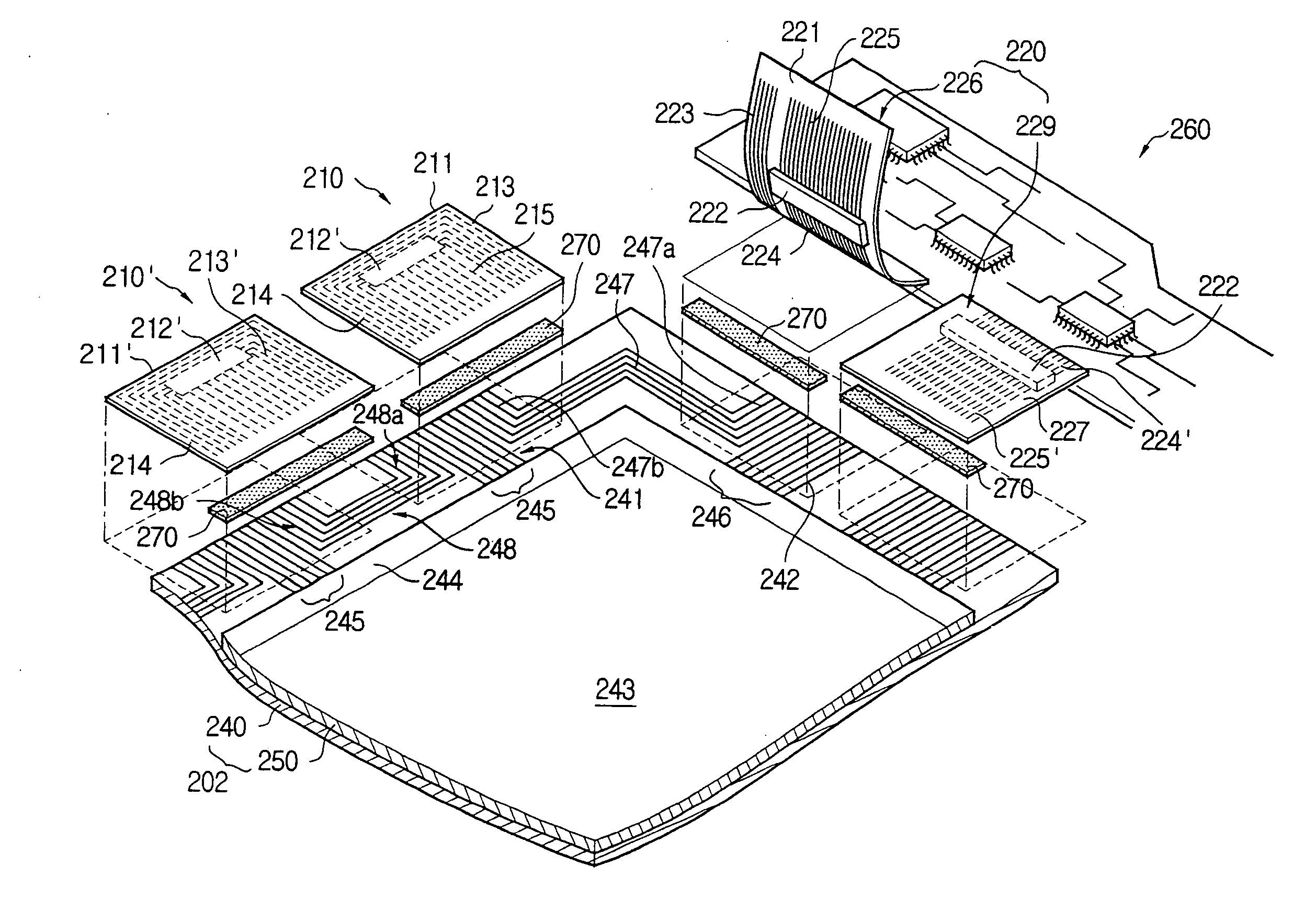
[0032]FIG. 2 is an exploded perspective view of the liquid crystal display according to a preferred embodiment of the present invention.

[0033] The liquid crystal display 601 comprises a liquid crystal display panel assembly 200, a back light assembly 300, a chassis 400 and a cover 500.

[0034] The back light assembly 300 is comprised of optical sheets 310, a light guiding plate 320, a lamp assembly 330, a light reflecting plate 340 and a mold frame as a receiving container.

[0035] Hereinafter, the liquid crystal display panel assembly 200 according to the present invention is described referring to the FIG. 3 and the ...


PUM


Abstract

A liquid crystal display of compact size is disclosed. The liquid crystal display has a tape carrier package and a single integrated PCB for processing a gate driving signal and data driving signal. The tape carrier package includes a base substrate, a gate driver IC formed on said base substrate, an input pattern formed on said base substrate that applies gate driving signals input from an external device to the gate driver IC, a first output pattern formed on said base substrate that outputs a first gate driving signal processed in said gate driver IC, and a second output pattern formed on said base substrate, that outputs a second gate driving signal bypassing the gate driver IC among the gate driving signals.

Description

BACKGROUND OF THE INVENTION [0001] 1. Field of the Invention [0002] The present invention relates to a tape carrier package for a compact size liquid crystal display (LCD), and more particularly to a tape carrier package (TCP) capable of receiving both of gate signal and data signal which are processed in a single integrated printed circuit board and transmitting the processed signals to an LCD panel and another TCP. Further, the invention relates to a liquid crystal display panel to which the tape carrier package is applied. [0003] 2. Description of the Related Art [0004] Generally, an LCD is a mostly used type of flat panel display. Especially, the small size, lighter weight and lower power consumption render the LCD to replace the traditional cathode ray tube (CRT). The LCD is currently used as a monitor for a lap-top computer and even for a desktop computer, gaining its popularity. [0005] As shown in FIG. 1, an LCD includes an LCD panel 101 and a light supply unit. The LCD panel...

Claims


Application Information

Patent Timeline
IPC IPC(8): G02F1/1335G02F1/13G02F1/13357G02F1/1345G02F1/136G02F1/1368G09F9/00H05K1/14H05K1/18H05K3/36
CPCG02F1/13452G09G3/3611G09G2300/0408Y10S345/905H05K1/189H05K3/361Y10S345/903G09G2300/0426G02F1/1345
Inventor KIM, SANG-SOOOH, CHOONG-SEOBPARK, JIN-HYEOKPARK, JIN-HOKIM, DONG-GYUPARK, YONG-EUNKANG, NAM-SOOLEE, GYU-SU
Owner SAMSUNG ELECTRONICS CO LTD
Features
  • Generate Ideas
  • Intellectual Property
  • Life Sciences
  • Materials
  • Tech Scout
  • Unparalleled Data Quality
  • Higher Quality Content
  • 60% Fewer Hallucinations
Learn More