Microscope and sample observation method

a microscope and sample technology, applied in the field of microscopes and sample observation methods, can solve the problems that the inspection of semiconductor devices requires a great deal of effort and time, and the inspection of semiconductor devices with sils has not yet been put to practical use in the field of semiconductor device inspection, so as to achieve the effect of focusing and aberration correction quickly and surely

Active Publication Date: 2005-09-01
HAMAMATSU PHOTONICS KK
View PDF32 Cites 29 Cited by
  • Summary
  • Abstract
  • Description
  • Claims
  • Application Information

AI Technical Summary

Benefits of technology

[0016] As a specific correction method, the microscope is preferably configured so that the controlling means comprises a first focusing table and a first aberration correction table corresponding to the first correction condition, and a second focusing table and a second aberration correction table corresponding to the second correction condition. Similarly, the sample observation method is preferably configured so that the first correction step

Problems solved by technology

The method of performing the observation in high resolution with the electron microscope after the inspection with light as described above has a problem that the inspection of semiconductor device requires a great deal of effort and time, for example, because of compli

Method used


Image

  • Microscope and sample observation method
  • Microscope and sample observation method
  • Microscope and sample observation method

Examples


Embodiment Construction

[0041] Preferred embodiments of the microscope and the sample observation method according to the present invention will be described below in detail with reference to the drawings. In the description of drawings the same elements will be denoted by the same reference symbols, without redundant description. It is also noted that dimensional ratios in the drawings do not always agree with those in the description.

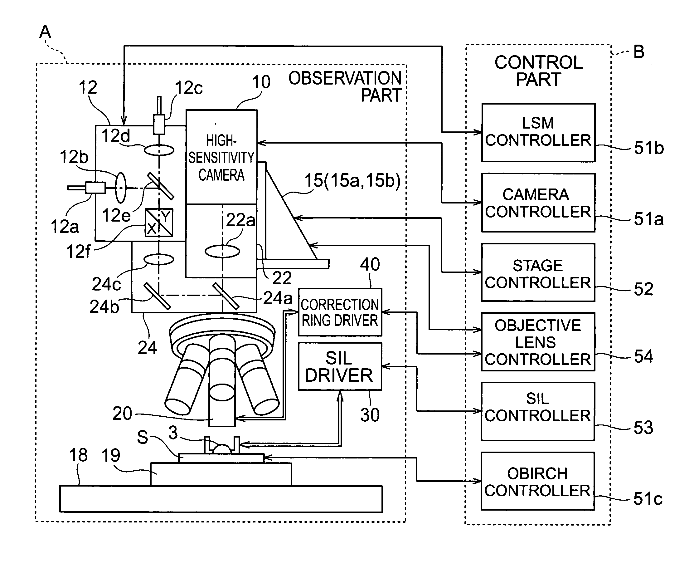
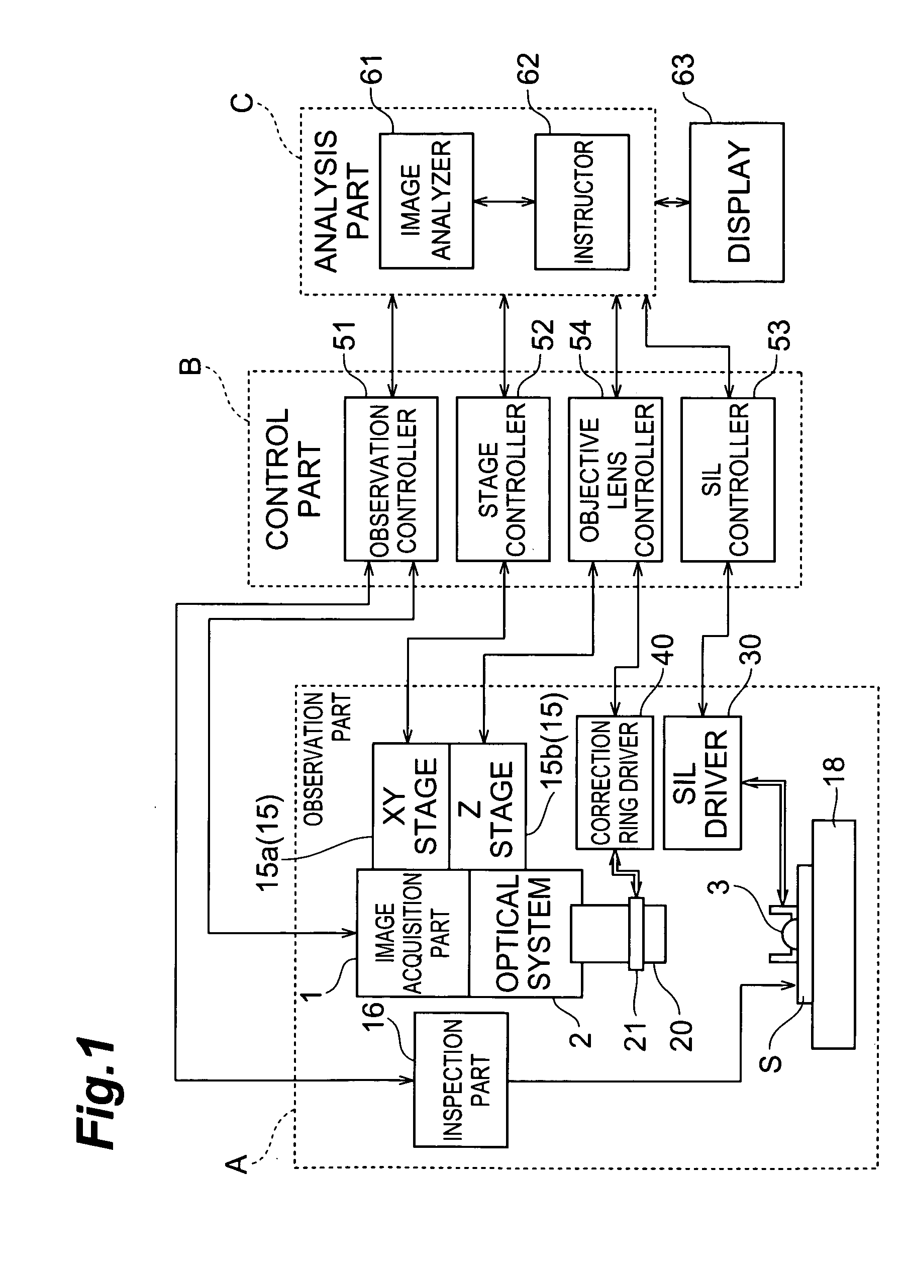
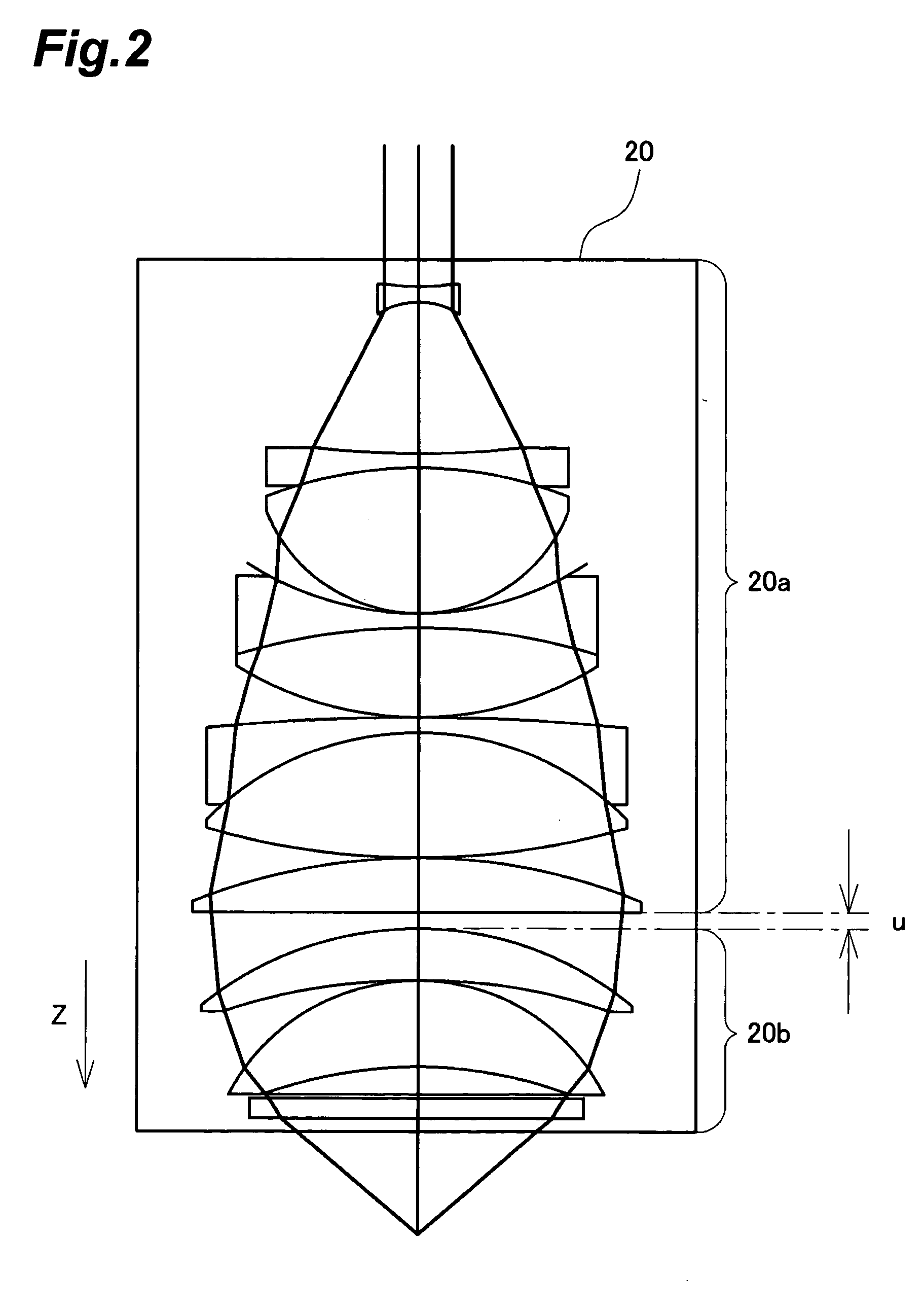
[0042] First, a basic configuration of a semiconductor inspection apparatus being a microscope according to the present invention will be described. FIG. 1 is a block diagram schematically showing a configuration of an embodiment of the semiconductor inspection apparatus according to the present invention. The present apparatus is an inspection device adapted for a semiconductor device S, for example, in which a circuit pattern consisting of transistors, interconnections, etc. is formed on a device surface, as a sample of an inspected object (observed object), and is config...


PUM


Abstract

For a semiconductor device S as an inspected object, there are provided an image acquisition part 1, an optical system 2 including an objective lens 20, and a solid immersion lens (SIL) 3 movable between an insertion position including an optical axis from the semiconductor device S to the objective lens 20 and a standby position off the optical axis. Then observation is carried out in two control modes consisting of a first mode in which the SIL 3 is located at the standby position and in which focusing and aberration correction are carried out based on a refractive index no and a thickness to of a substrate of the semiconductor device S, and a second mode in which the SIL 3 is located at the insertion position and in which focusing and aberration correction are carried out based on the refractive index no and thickness t0 of the substrate, and a refractive index n1, a thickness d1, and a radius of curvature R1 of SIL 3. This provides a microscope and a sample observation method capable of readily performing observation of the sample necessary for an analysis of microstructure or the like of the semiconductor device.

Description

BACKGROUND OF THE INVENTION [0001] 1. Field of the Invention [0002] The present invention relates to a microscope used for observing a sample such as a semiconductor device at a predetermined observation plane and through the sample, and a sample observation method. [0003] 2. Related Background Art [0004] In recent years, many of semiconductor devices are being fabricated using face down bonding and flip chip bonding with a device surface (active circuit surface) at the bottom side of a substrate. In inspection of such semiconductor devices, it is sometimes difficult to expose the device surface of the substrate without disassembling a package, depending upon a type of the package and a mounting direction. Even in cases where a device surface of a substrate mounted not using the flip chip mounting can be exposed, but where semiconductor devices are highly integrated or multilayered, it is becoming hard to observe interconnections, devices, etc. in lower layers. Correspondingly, a me...

Claims


Application Information

Patent Timeline
IPC IPC(8): G02B21/00G02B21/33
CPCG02B21/0016Y10S359/90G02B21/33G02B21/00
Inventor TERADA, HIROTOSHIARATA, IKUOTOKIWA, MASAHARUTANABE, HIROSHISAKAMOTO, SHIGERU
Owner HAMAMATSU PHOTONICS KK
Why Eureka
Try Eureka