Semiconductor device

Inactive Publication Date: 2005-09-01
PANASONIC CORP
View PDF13 Cites 36 Cited by
  • Summary
  • Abstract
  • Description
  • Claims
  • Application Information

AI Technical Summary

Benefits of technology

[0025] An object of the present invention is to provide a semiconductor memory device which performs stable reading operation with less deterioration in capability.
[0063] According to this structure, the load capacitor circuit is shared by memory cells so that a cell area can be small. That is, the circuit scale is decreased so as to make high integration easy.

Problems solved by technology

However, according to the conventional technology, the first problem is that a storing capability (a retention characteristic) of the ferroelectric capacitors in the nonvolatile RAM is deteriorated by aged changes lowering a reliability of operations.
Further, the second problem is that it is difficult to integrate in large scale in the case where circuit elements having nonvolatile RAMs are integrated in large scale.
The storing capacity (a retention characteristic) of the ferroelectric capacitors is deteriorated by polarization when a voltage is continued to be applied, causing operational malfunctions.
Explaining the first problem in other words, as shown in FIG. 5, there is a possibility that the ferroelectric built-in latch circuit to which a plurality of ferroelectric capacitors is connected to storage nodes deteriorates its capacity by a thermal history of which the data is being held depending on a state of polarization, and cause an unstable reading operation.
Because it is difficult to perform stable reading operation.
Therefore, it has a large area of memory cell so that a high integration is difficult.

Method used


Image

  • Semiconductor device
  • Semiconductor device
  • Semiconductor device

Examples


first embodiment

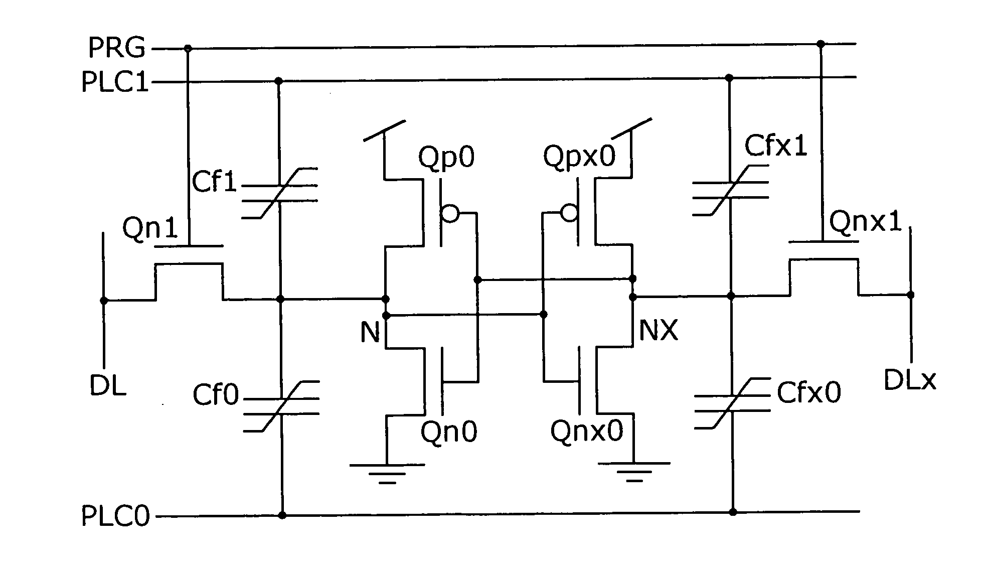
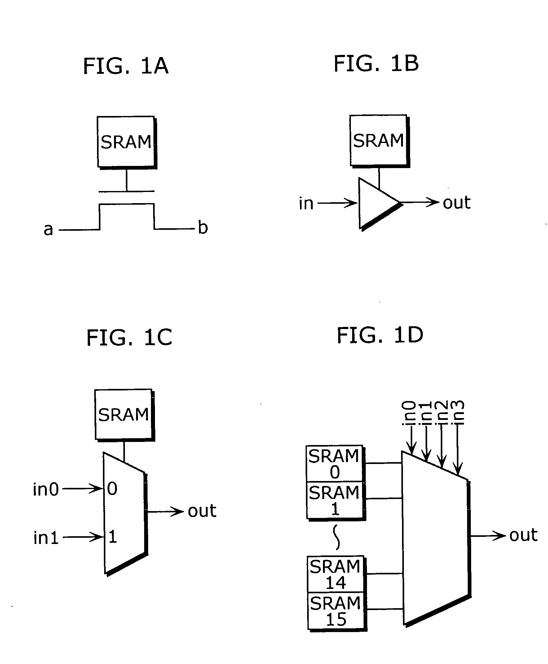
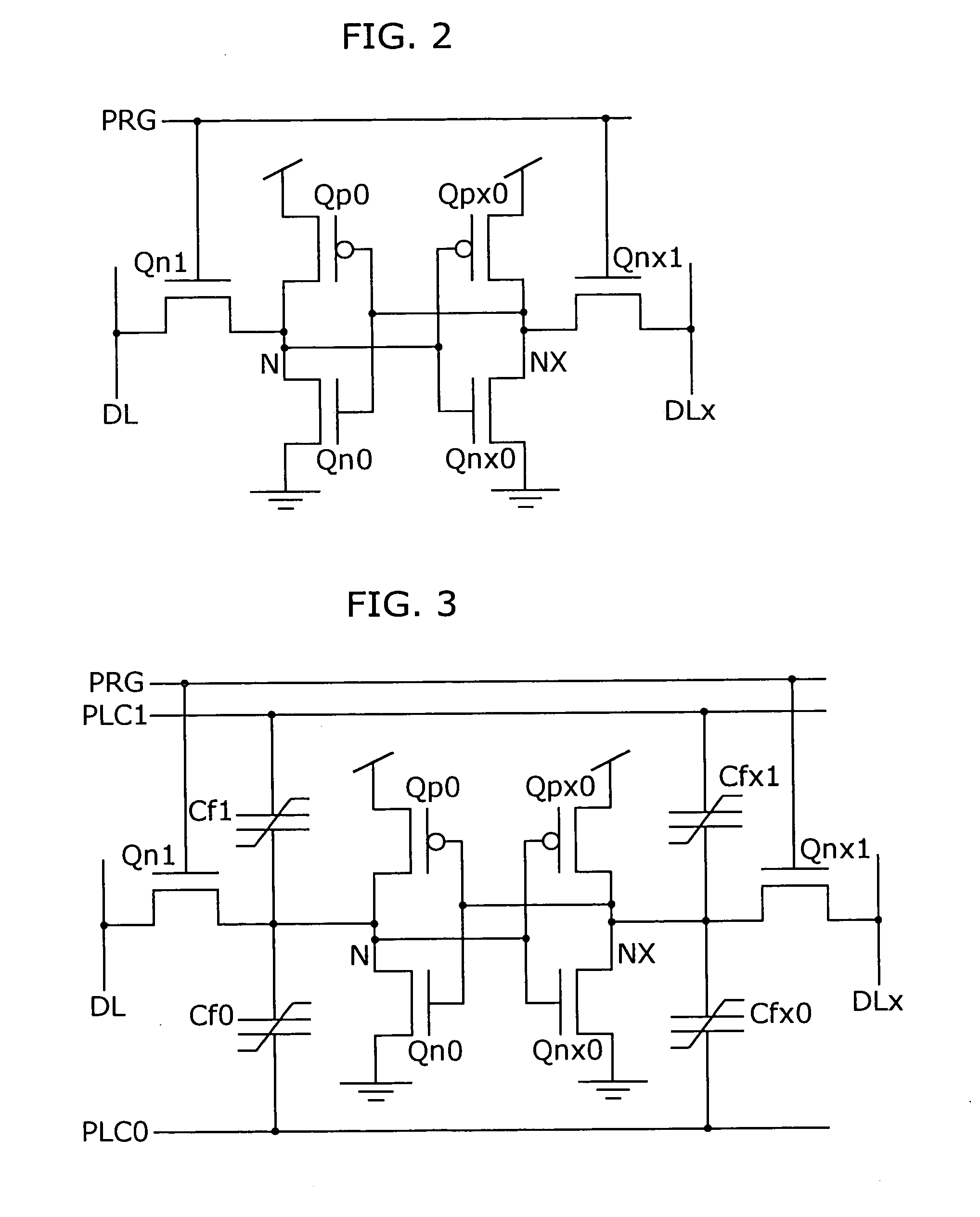
[0109] Here, a reconfigurable logic circuit in the first embodiment of the present invention is explained. FIGS. 6A to 6D are diagrams showing circuit elements used in a reconfigurable logic circuit.

[0110]FIG. 6A shows a circuit element which functions as a pass transistor. The pass transistor has nonvolatile memory cells NVC (a) and NVC (b), a switch circuit SW, a SRAM and a transistor. The NVC (a) is a nonvolatile memory cell which uses ferroelectric capacitor as a memory cell, and holds data which is a part of circuit configuration information. The NVC (b) is a similar memory cell and holds data that is a part of other circuit configuration information. The switch circuit SW selects one of the nonvolatile memory cells NVC (a) and NVC (b) in accordance with a reconfiguration control signal RC, and connects the selected nonvolatile memory cell to the SRAM only when the configuration is performed. The SRAM is a latch circuit which reads data from and writes data to the nonvolatile ...

second embodiment

[0143] It is explained about a ferroelectric incorporated latch circuit according to the second embodiment of the present invention. FIG. 19 shows a circuit diagram of the second embodiment. In the latch circuit, two inverters INV0 and INV1 are connected in cross-couple, and data is written and read from bit lines BL and XBL by access transistors Q0 and XQ0 whose gates are controlled by the world line WL. Also, two data storage ferroelectric capacitors CF0 and XCF0 and two load ferroelectric capacitors CF1 and XCF1 are respectively connected to the two storage nodes N0 and XN0 in the latch circuit via the transistors Q1, XQ1, Q2 and XQ2 whose gates are controlled by the control lines EN0 and EN1. Theses connection nodes are available for grounding by the transistors Q3, XQ3, Q4 and XQ4 whose gates are controlled by the control lines EQ0 and EQ1. One side of electrodes of the CF0 and XCF0 is respectively connected to the plate line PL0 and one side of electrodes of the CF1 and XCF1 i...

third embodiment

[0153]FIG. 25 shows a ferroelectric built-in latch circuit diagram according to a third embodiment of the present invention. In the present embodiment, there are two memory cells composed of a latch circuit and data storage ferroelectric capacitors and a load cell including load ferroelectric capacitors is shared. In FIG. 25, an element to which a number (0) is attached forms a first memory cell and an element to which a number (1) is attached forms a second memory cell. The latch circuit is formed by connecting two inverters INV0 (0, 1) and INV1 (0, 1) in cross couple. In the latch circuit, data is written in and read from the bit lines BL and XBL by the access transistors Q0 (0, 1) and XQ0 (0, 1) whose gates are controlled by the word line WL (0, 1). Two data storage ferroelectric capacitors CF0 (0, 1) and XCF0 (0, 1) are respectively connected to the two storage nodes N0 (0, 1) and XN0 (0, 1) of the latch circuit via the transistors Q1 (0, 1) and XQ1 (0, 1) whose gates are contro...


PUM


Abstract

The semiconductor device of the present invention includes a volatile latch circuit which holds data, a nonvolatile ferroelectric capacitor circuit which holds data, and a switch circuit which connects and disconnects between the latch circuit and the ferroelectric capacitor circuit.

Description

BACKGROUND OF THE INVENTION [0001] (1) Field of the Invention [0002] The present invention relates to a high-speed reconfigurable logic circuit in which ferroelectric capacitors are included. [0003] (2) Description of the Related Art [0004] In recent years, there has been an increase in need that “debugging to be completed until the shipping in accordance with sophistication of processing details of LSI” or that “it is wished to correct a bug found after the shipping”. Following that, a demand for an electronically reconfigurable logic circuit has been increased. There are commercialized circuits such as a Field Programmable Gate Array (FPGA) and a Programmable Logic Device (PLD). [0005] A conventional reconfigurable logic circuit is explained with references to drawings. FIGS. 1A to 1D are diagrams showing circuit elements used in a reconfigurable logic circuit. FIG. 1A shows a configuration of a pass transistor. A conduction / non-conduction between a terminal “a” and a terminal “b”...

Claims


Application Information

Patent Timeline
IPC IPC(8): G11C11/22
CPCG11C11/22G11C14/0072
Inventor KATO, YOSHIHISA
Owner PANASONIC CORP
Why Eureka
Try Eureka