Electron beam treatment apparatus

Inactive Publication Date: 2005-09-08
APPLIED MATERIALS INC
View PDF7 Cites 1 Cited by
  • Summary
  • Abstract
  • Description
  • Claims
  • Application Information

AI Technical Summary

Benefits of technology

[0007] In light of the above, there is a need to ov

Problems solved by technology

Fabrication of integrated devices, for example, and without limitation, semiconductor integrated devices, is complicated and, due to increasingly stringent requirements on device designs due to demands for greater device speed, fabrication is becoming ever more complicated.
In the production of advanced integrated circuits that have minimum feature sizes of 0.13 μm and below, problems of RC delay, power consumption, and crosstalk become significant.
Temperature uniformity across a wafer or substrate during treatment using a prior art electron beam treatment apparatus is about ±10° C., and this is problematic in terms of process uniformity.

Method used


Image

  • Electron beam treatment apparatus
  • Electron beam treatment apparatus
  • Electron beam treatment apparatus

Examples


Embodiment Construction

[0014] Advantageously, one or more embodiments of the present invention provide an electron beam treatment apparatus that provides less than about 8° C. max / min temperature uniformity during electron beam treatment across a 300 mm wafer or substrate at a wafer or substrate set point temperature of about 400° C.

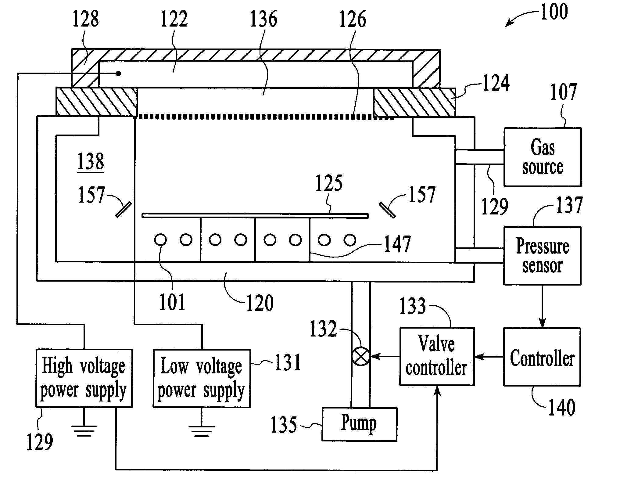
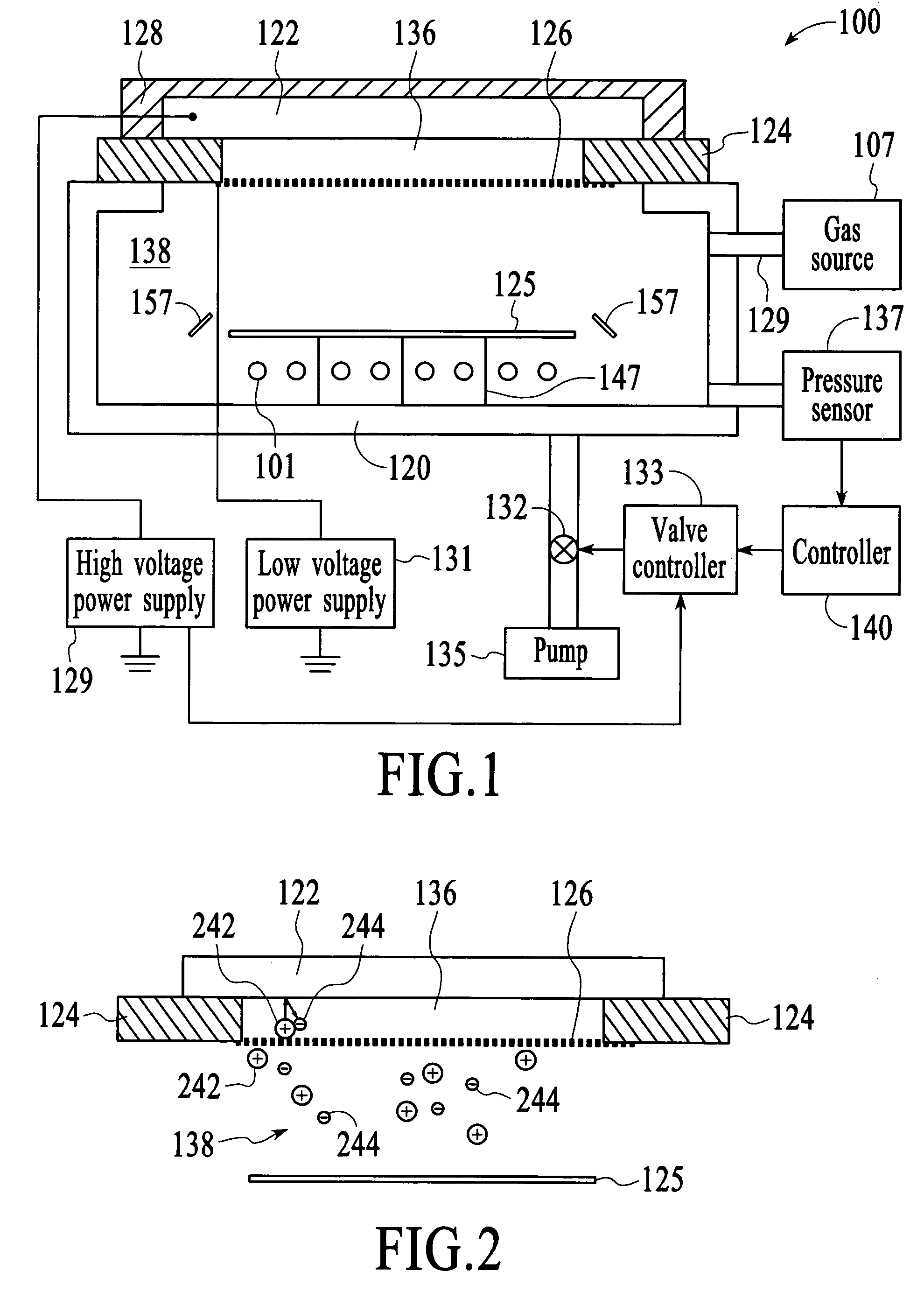
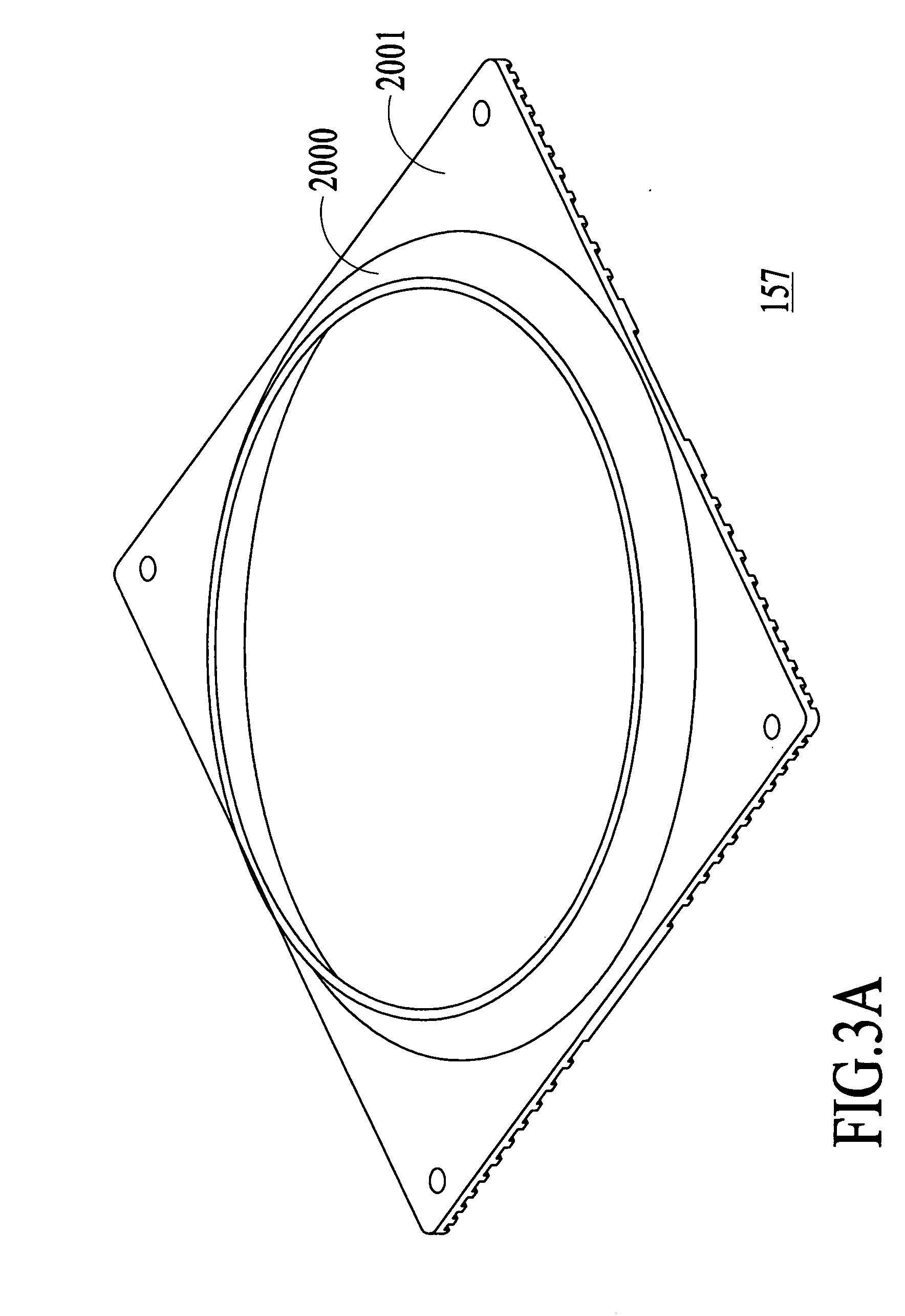
[0015]FIG. 1 shows a schematic diagram of a partial cross sectional view of large area electron beam source, electron beam treatment apparatus 100 (e-beam apparatus 100) that is fabricated in accordance with one or more embodiments of the present invention. Such an e-beam treatment apparatus is available from Applied Materials, Inc. of Santa Clara, Calif. As shown in FIG. 1, e-beam apparatus 100 includes array 101 of quartz halogen lamps for heating a substrate or a wafer, which array is surrounded by lamp heat shield 157 to provide substantial temperature uniformity across a wafer.

[0016] As further shown schematically in FIG. 1, substrate 125 is held over array 101 of lamps...


PUM


Abstract

One embodiment of the present invention is an electron beam treatment apparatus that includes: (a) an array of lamps that output radiation; (b) a support mechanism adapted to support a substrate at a treatment position above the lamps; and (c) a lamp heat shield, disposed above the array, having a radiation absorption portion adapted to absorb radiation from at least a portion of the array, and a radiation reflection portion adapted to reflect radiation from at least a portion of the array towards the substrate when disposed at the treatment position.

Description

TECHNICAL FIELD OF THE INVENTION [0001] One or more embodiments of the present invention pertain to apparatus for electron beam treatment used to fabricate integrated circuit devices. BACKGROUND OF THE INVENTION [0002] Fabrication of integrated devices, for example, and without limitation, semiconductor integrated devices, is complicated and, due to increasingly stringent requirements on device designs due to demands for greater device speed, fabrication is becoming ever more complicated. For example, integrated circuit geometries have decreased in size substantially since such devices were first introduced several decades ago. Since then, integrated circuits have generally followed a two year / half-size rule (often called Moore's Law), which means that the number of devices on a chip doubles every two years. Today's fabrication facilities are routinely producing devices having 0.13 μm feature sizes, and tomorrow's facilities soon will be producing devices having even smaller feature...

Claims


Application Information

Patent Timeline
IPC IPC(8): H01J37/30
CPCH01J37/20H01J37/317H01L21/67115H01J2237/316H01J2237/3165H01J2237/2001
Inventor QUACH, DAVID H.ZHAO, JUN
Owner APPLIED MATERIALS INC
Why Eureka
Try Eureka