Method and system of characterizing a device under test

a technology of voltage noise and device, applied in the direction of resistance/reactance/impedence, measurement devices, instruments, etc., can solve the problems of over-constrainting the design of the power delivery network, power delivery systems are simultaneously becoming increasingly difficult to design, measure and characterize, and require large currents, etc., to correctly determine the voltage noise of the device under test

Inactive Publication Date: 2005-09-08
COLE J BRADFORD
View PDF4 Cites 26 Cited by
  • Summary
  • Abstract
  • Description
  • Claims
  • Application Information

AI Technical Summary

Benefits of technology

[0010] It is therefore an object of this invention to more c

Problems solved by technology

Furthermore, the more quickly the electronic circuit draws current through the power delivery system, the wider the frequency bandwidth must be in order to maintain a given amount of transient voltage switching noise.
As electronic circuits operate at faster speeds, and as printed circuit boards and integrated circuits become more complex, they require larger amounts of current.
Therefore, the electrical performance of power delivery systems is becoming more critical to overall electronic system performance, and power delivery systems are simultaneously becoming increasingly challenging to design, measure, and characterize.
Although this technique is one commonly applied methodology to determine the electrical performance requirements of a power delivery network, it can be shown that this technique will always over-constrain the design of the power delivery network.
The result is a device that is more expensive to design, a design which takes longer to complete, and a product which take

Method used


Image

  • Method and system of characterizing a device under test
  • Method and system of characterizing a device under test
  • Method and system of characterizing a device under test

Examples


Embodiment Construction

[0038] Aside from the preferred embodiment or embodiments disclosed below, this invention is capable of other embodiments and of being practiced or being carried out in various ways. Thus, it is to be understood that the invention is not limited in its application to the details of construction and the arrangements of components set forth in the following description or illustrated in the drawings.

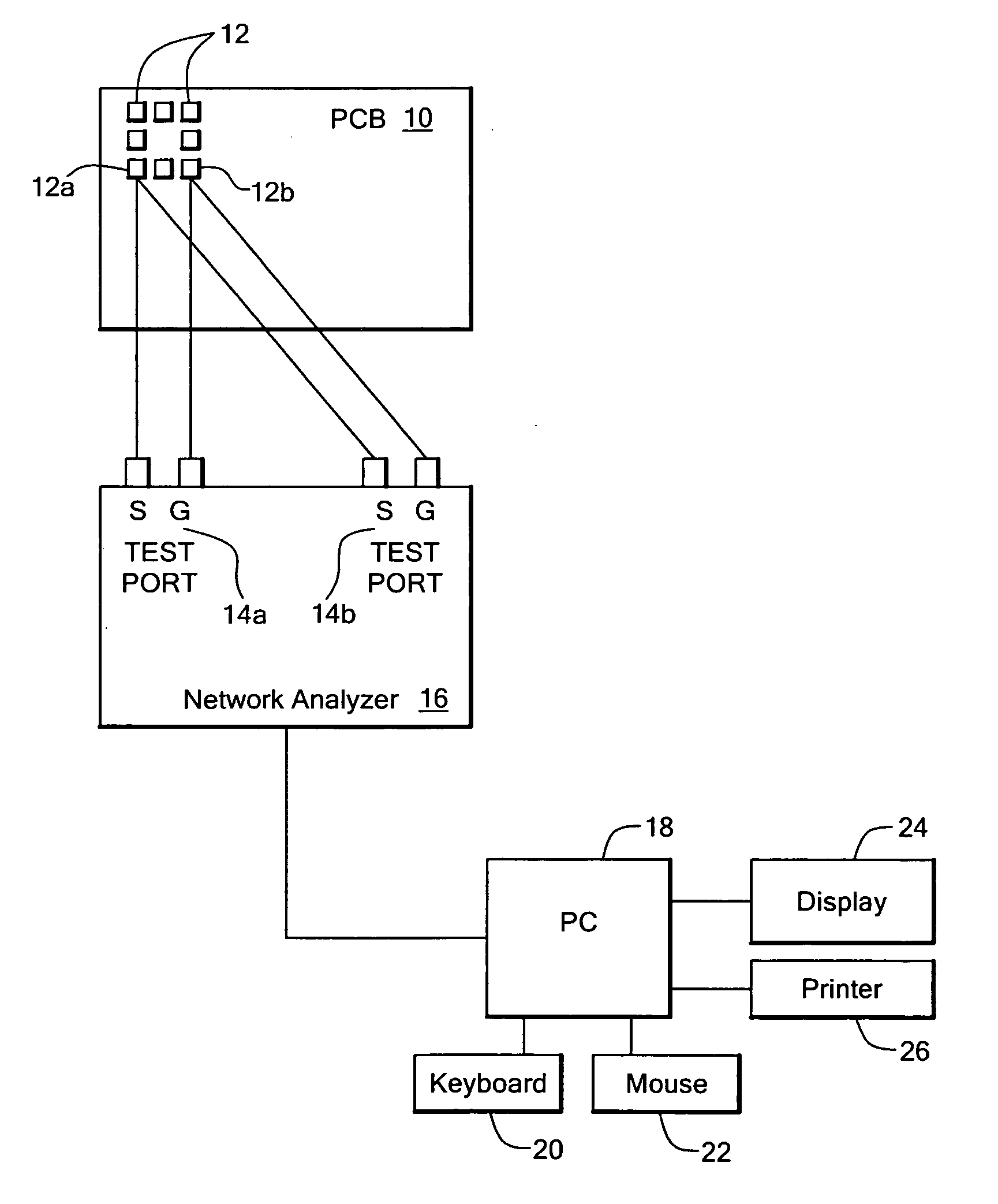
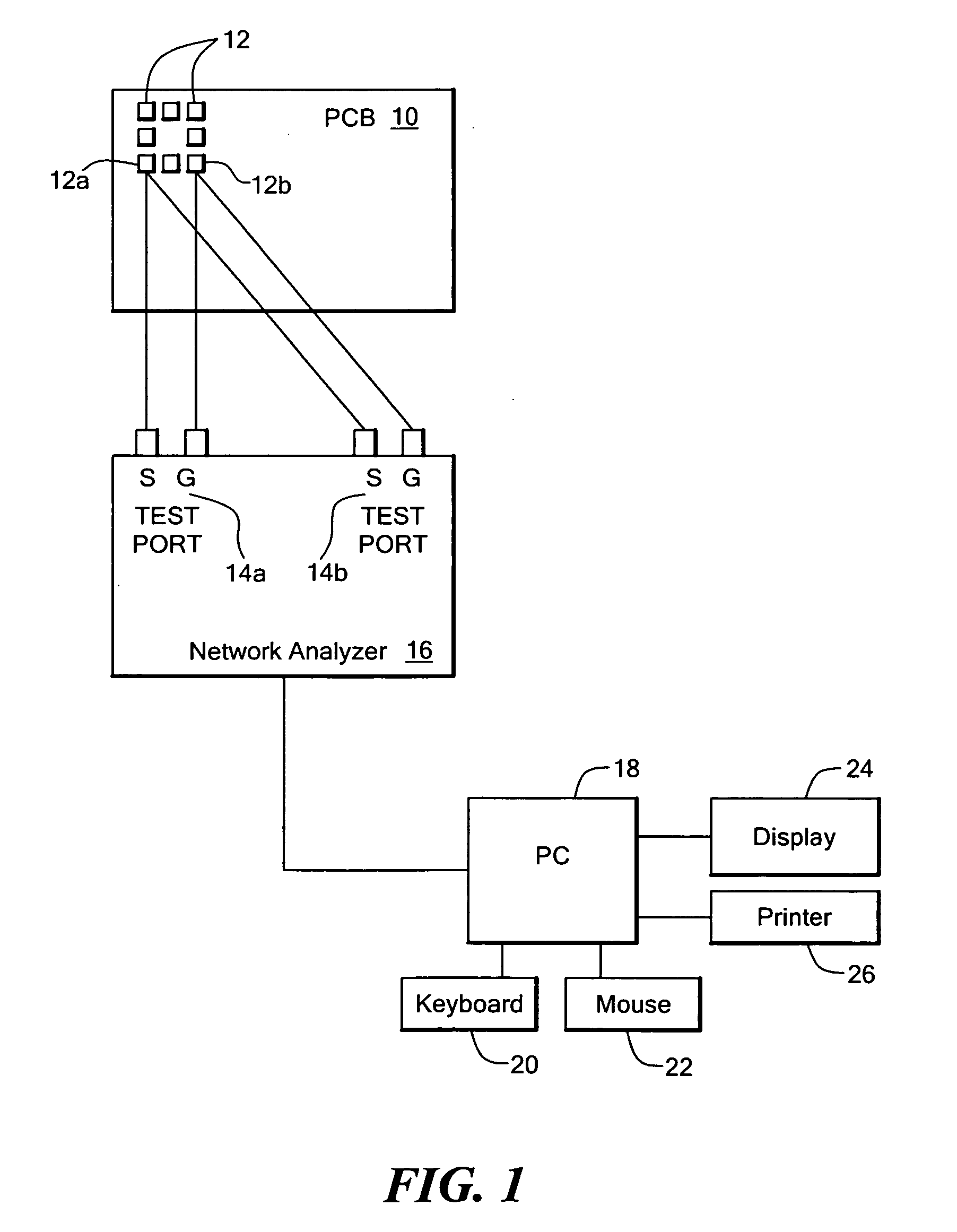
[0039]FIG. 1 shows a device under test 10 in the form of a printed circuit board. Other possible devices include integrated circuit packages and other electronic systems, devices, and components (e.g., interconnect components such as wire bonds and vias). Also, the “device” under test may be a digital representation of a physical device represented on a computer as is the case in the early design stages of a device when, for example, computer aided design software is used to design and model a new printed circuit board.

[0040] Pads 12 are where an electronic chip or package might be mount...


PUM


Abstract

A system and method of characterizing a device under test wherein a signal is injected into the device under test, the response to the injected signal is measured to determine the impedance of the device under test in the frequency domain, the impedance is converted to the time domain, and the voltage noise of the device under test is calculated based on the impedance of the device under test in the time domain.

Description

FIELD OF THE INVENTION [0001] This invention relates to a method and system of characterizing a device under test to determine the voltage noise of a device and to otherwise evaluate the power delivery network and signal return planes of electronic systems. BACKGROUND OF THE INVENTION [0002] The power delivery systems (e.g., the network and signal return planes) of printed circuit boards, integrated circuit packages, and other systems, devices, and components, (e.g., interconnect components such as wire bonds and vias), are routinely tested for voltage noise. The power delivery network of a printed circuit board, for example, consists of Vcc (supply voltage) pads and ground pads and the power plane and ground plane, and / or conductive traces in or on the printed circuit board which lead to other pads or to a connector or the like. In general, power delivery networks transfer electrical power from a power supply to an electronic circuit. Generally speaking, for a given supply voltage,...

Claims


Application Information

Patent Timeline
IPC IPC(8): G01R27/04G01R27/28
CPCG01R27/28
Inventor COLE, J. BRADFORD
Owner COLE J BRADFORD
Why Eureka
Try Eureka