Display device

a display device and display technology, applied in static indicating devices, instruments, non-linear optics, etc., can solve the problems of insufficient time for writing gray scale voltages from video lines into sub-pixels, difficult routing of interconnection wiring, etc., and achieve the effect of reducing time and improving definition

Active Publication Date: 2005-09-15
PANASONIC LIQUID CRYSTAL DISPLAY CO LTD +1
View PDF6 Cites 17 Cited by
  • Summary
  • Abstract
  • Description
  • Claims
  • Application Information

AI Technical Summary

Benefits of technology

[0018] The present invention is capable of securing sufficient time for writing gray scale voltages into each of the sub-pixels in a display device employing a time-division multiplexed driving even when the display area is configured so as to provide a higher definition.

Problems solved by technology

In the case of this higher-definition display panel, the sub-pixel pitch is naturally reduced, the number of video lines for supplying gray scale voltages to respective sub-pixels is increased, and consequently, the routing of interconnection wiring becomes difficult.
However, the present inventors have found out that there is a problem in that time for writing gray scale voltages from video lines into sub-pixels becomes insufficient in this time-division multiplexed driving method when the liquid crystal display panel is configured so as to provide a higher definition, since writing time T available for writing gray scale voltages into three sub-pixels in a time-division multiplexed fashion is usually divided into three equal intervals for three sub-pixels, respectively.

Method used


Image

  • Display device
  • Display device
  • Display device

Examples


example 1

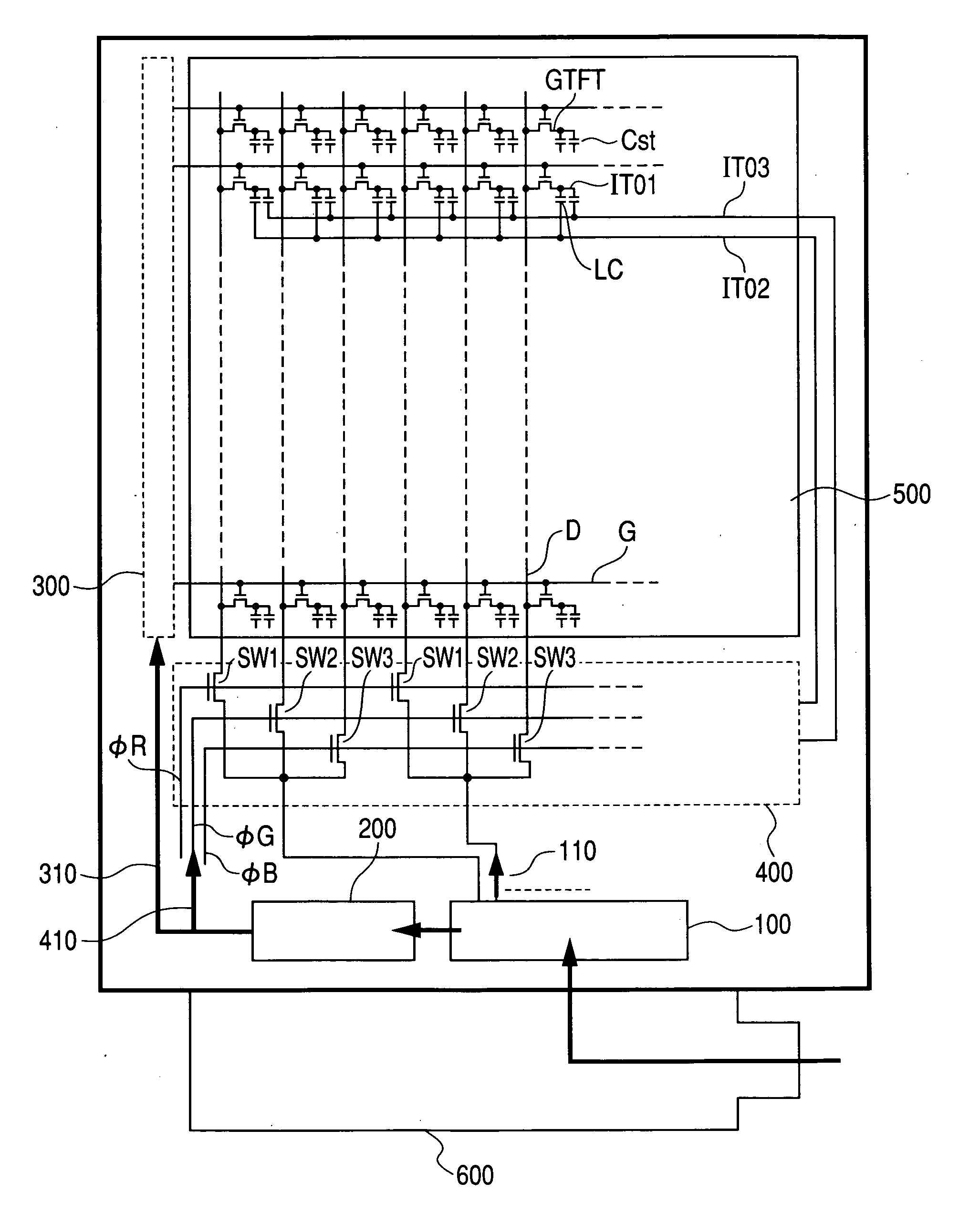
[0030]FIG. 1 is a block diagram illustrating a rough configuration of a liquid crystal display module in accordance with Example 1 of the present invention. The liquid crystal display module of Example 1 is a polysilicon type liquid crystal display module which uses polysilicon as semiconductor layers of thin film transistors (TFTs).

[0031] The liquid crystal display module of Example 1 comprises a drain driver (a video line drive circuit) 100, a power supply circuit 200, a gate scanning circuit 300, a drain line selection switching circuit 400, and a display section 500. The drain line selection switching circuit 400 comprises a plurality of the circuits shown in FIG. 7. The display section 500 includes a plurality (for example, 240×320××3) of sub-pixels arranged in a matrix fashion, a plurality of video lines D (also called drain lines) for supplying video signal voltages to respective sub-pixels, and a plurality of scanning lines G (also called gate lines) for supplying scanning ...

example 2

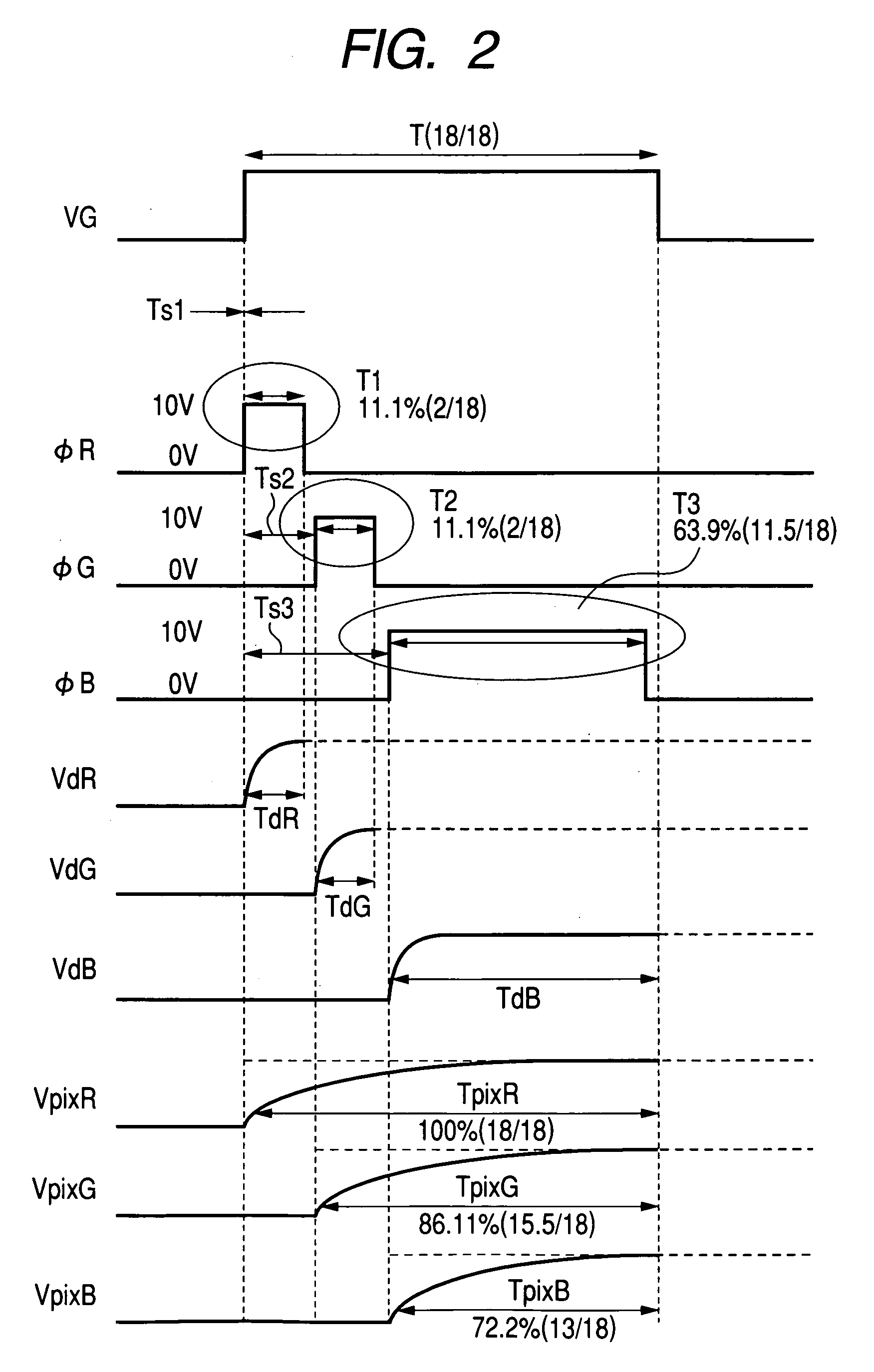
[0070] In Example 1, times during which the video line selection pulses φR, φG and φB stay at the H level are not equal to each other in duration, but are made unequal to each other. To be concrete, T1=T23.

[0071] Therefore, there is concern that the video-line writing times TdR and TdG for writing gray scale voltages into corresponding ones of the video lines D after the switching elements SW1 and SW2 being turned on might be insufficient in some cases. This Example 2 solves this problem.

[0072]FIG. 3 is an illustration for explaining a time-division multiplexed driving method of this Example 2. As shown in FIG. 3, in this Example 2, times during which the video line selection pulses φR, φG and φB stay at the H level are not equal to each other in duration, but are made unequal to each other. In addition to this, voltages VG1 and VG2 corresponding to the H levels of the video line selection pulses φR and φG, respectively, are selected to be higher than a voltage VG3 corresponding t...

example 3

[0079] As in the case of Example 2, this Example 3 also solves the problem of possible insufficiency of the video-line writing times TdR and TdG for writing gray scale voltages into corresponding ones of the video lines D after the switching elements SW1 and SW2 are turned on.

[0080] This Example 3 selects the ON-currents of the thin film transistors forming the switching elements SW1 and SW2 to be larger than the ON-current of the thin film transistor forming the switching element SW3. The voltages VdR, VdG and VdB rise when the video line selection pulses φR, φG and φB go to the H levels, respectively. In this Example 3, since the ON-currents of the thin film transistors forming the switching elements SW1 and SW2 are made larger than the ON-current of the thin film transistor forming the switching element SW3, the voltages VdR and VdG rise more sharply than the voltage VdB like in the portions designated B in FIG. 3. This prevents the video-line writing times TdR and TdG from beco...


PUM

PropertyMeasurementUnit
gray scale voltagesaaaaaaaaaa
voltagesaaaaaaaaaa
Tmaaaaaaaaaa

Abstract

A display device includes sub-pixels, video lines, a drive circuit and switch groups. The video lines are divided into plural blocks each composed of m video lines, m being an integer of 2 or more. The drive circuit outputs m gray scale voltages time-sequentially. Each of the switch groups corresponding to one of the blocks is composed of first to mth switches, receives the m gray scale voltages from the drive circuit, and then supplies them to the m video lines in a time-division multiplexed fashion. The mth switch is turned on last during a writing time for writing. the m gray scale voltages into the sub-pixels, and Tq<Tm, where Tm and Tq are times during which the mth switch and a qth switch of the first to (m−1)th switches are turned on, respectively, and q is an integer of from 1 to ( m−1).

Description

CLAIM OF PRIORITY [0001] The present application claims priority from Japanese application serial no. 2004-065054, filed on Mar. 9, 2004, the content of which is hereby incorporated by reference into this application. BACKGROUND OF THE INVENTION [0002] The present invention relates to a display device, and in particular to a technique useful for application to a display device employing a time-division-multiplexed driving. TFT (Thin Film Transistor) type liquid crystal modules are widely used as displays for portable equipment such as notebook personal computers or the like. Especially, liquid crystal display modules provided with a small-sized liquid crystal display panel are used as displays for portable equipment always carried such as mobile phones, for example. [0003] Usually there are as many outputs of a drain driver (also called a video line drive circuit) for driving a liquid crystal display panel as there are video lines (also called drain lines) of the liquid crystal disp...

Claims


Application Information

Patent Timeline
Patent Type & Authority Applications(United States)
IPC IPC(8): G02F1/133G02F1/1362G09G3/20G09G3/36
CPCG02F1/1345G02F1/13454G09G3/3648G09G2320/0252G09G2310/08G09G3/3688G09G2310/0235G09G2300/0408
Inventor GOTO, KAZUTAKAASUMA, HIROAKIHASEGAWA, ATSUSHI
Owner PANASONIC LIQUID CRYSTAL DISPLAY CO LTD
Why Eureka
Try Eureka