Semiconductor module with heat sink and method thereof

a technology of semiconductors and heat sinks, applied in the field of semiconductor modules, can solve problems such as reducing the efficiency of heat radiation

Active Publication Date: 2005-09-15
SAMSUNG ELECTRONICS CO LTD
View PDF26 Cites 103 Cited by
  • Summary
  • Abstract
  • Description
  • Claims
  • Application Information

AI Technical Summary

Problems solved by technology

Further, a first space S1 between the PCB 11 and the heat sink 13 may be be

Method used


Image

  • Semiconductor module with heat sink and method thereof
  • Semiconductor module with heat sink and method thereof
  • Semiconductor module with heat sink and method thereof

Examples


Embodiment Construction

[0024] Hereinafter, exemplary embodiments of the present invention will be described in detail with reference to the accompanying drawings.

[0025] In the Figures, the same reference numerals are used to denote the same elements throughout the drawings.

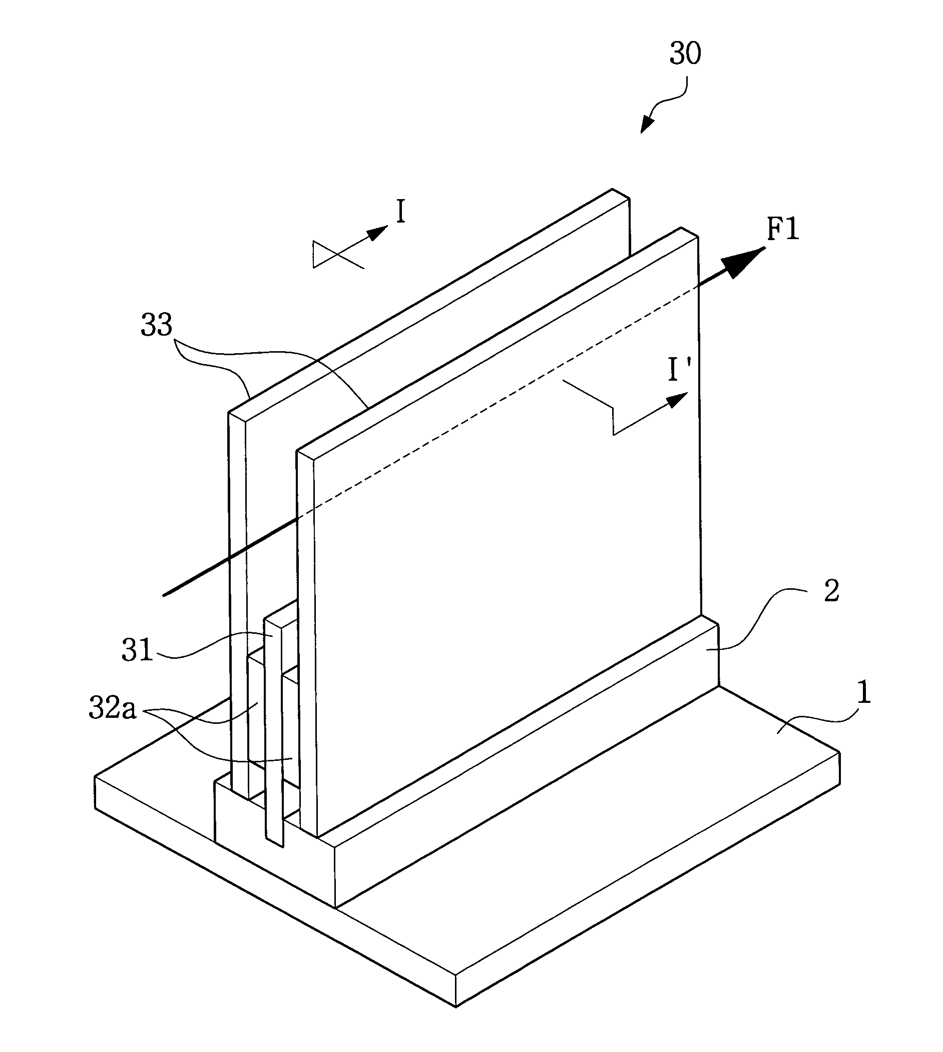
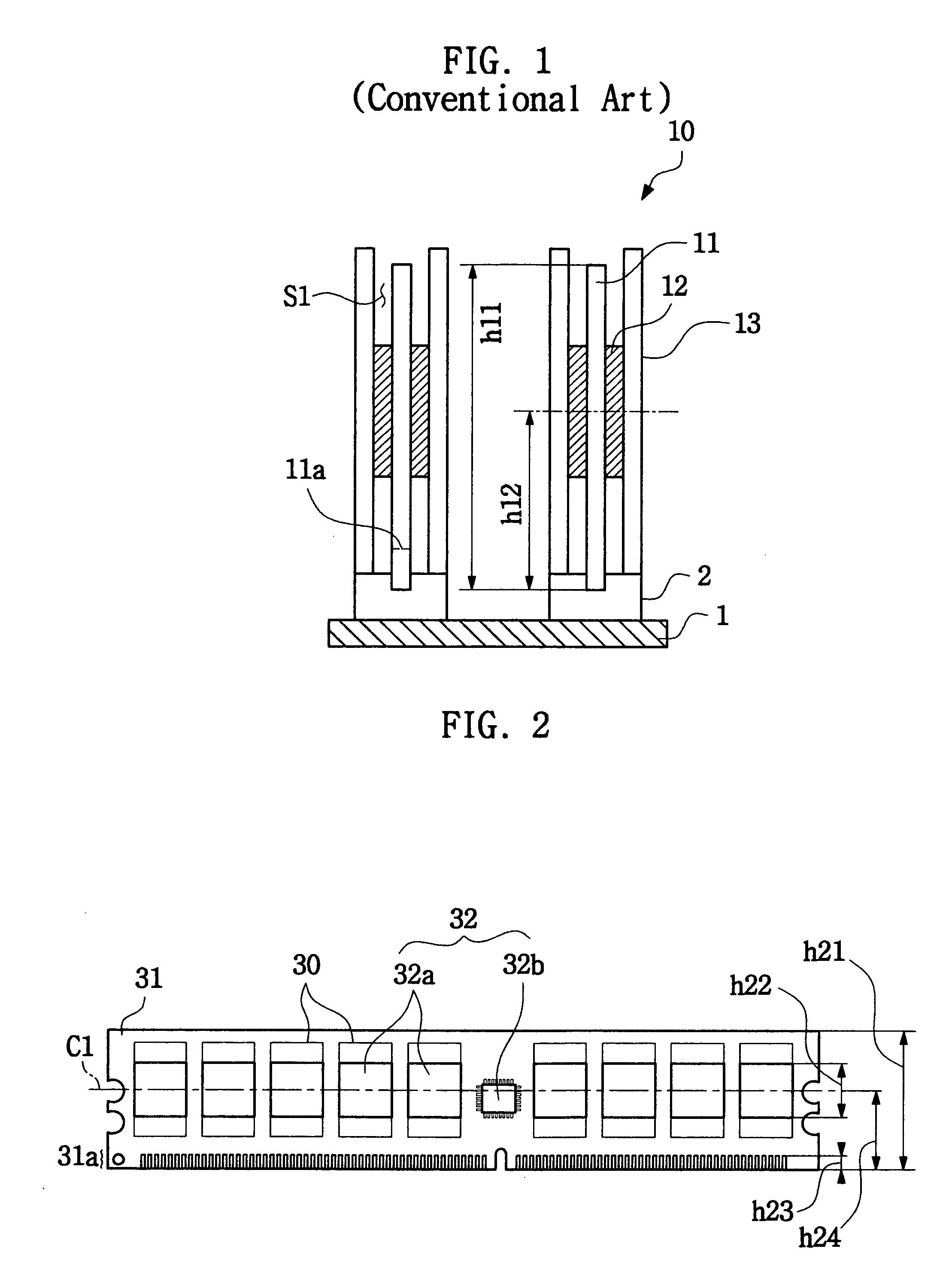
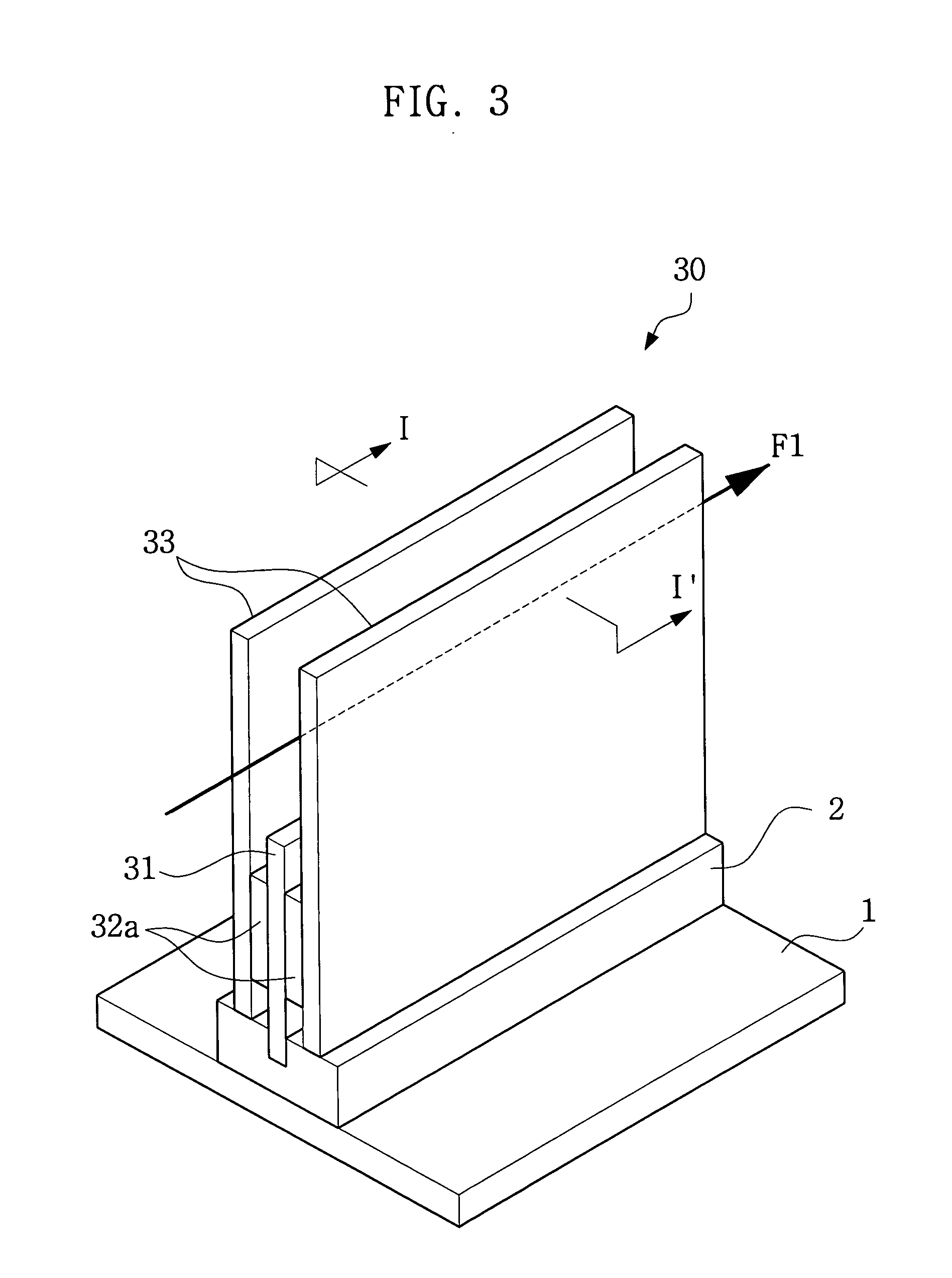
[0026]FIG. 2 illustrates a front-view of a printed circuit board (PCB) according to an exemplary embodiment of the present invention.

[0027] In an exemplary embodiment of the present invention, referring to FIG. 2, the PCB 31 may include semiconductor devices 32a within a semiconductor module 30. The semiconductor device 32 may be mounted on the PCB 31. The PCB 31 may include a connection terminal portion 31a which may provide an electrical connection with a module socket (not shown) at the lower end thereof. The semiconductor device 32 may include a data storage element, for example a memory device 32a, and a phase lock loop (PLL) circuit 32b. A condenser chip may be mounted on the PCB 31. Condenser chips are well known in the art an...


PUM


Abstract

A semiconductor module, including a semiconductor device mounted on a printed circuit board (PCB), the PCB having an electrical connection to the semiconductor module, and a heat sink in direct contact with the semiconductor device, the heat sink being formed with a first end and a second end, the first end and the second end being formed with different heights, wherein the semiconductor module allows air flow to pass through the semiconductor module, radiating heat away from the heat sink. Another semiconductor module, including a semiconductor device mounted on a PCB, a heat sink in direct contact with the semiconductor device, the heat sink having a first portion and a second portion, wherein the first portion has a flat shape and is in direct contact with the semiconductor device and the second portion has a corrugated shape and is not in contact with the semiconductor device, wherein the semiconductor module allows air flow to pass through the semiconductor module, radiating heat away from the heat sink.

Description

CROSS REFERENCE TO RELATED APPLICATIONS [0001] This U.S. non-provisional application claims priority under 35 U.S.C. §119 of Korean Patent Application No. 2004-17425, filed on Mar. 15, 2004, the entire contents of which are incorporated herein by reference.BACKGROUND OF THE INVENTION [0002] 1. Field of the Invention [0003] The present invention relates generally to a semiconductor module, and more particularly, to a semiconductor module including a heat sink and method thereof. [0004] 2. Description of the Related Art [0005] Recently, semiconductor products have generally become more integrated. A semiconductor module may include a plurality of semiconductor devices mounted on a printed circuit board (PCB). A conventional semiconductor module may include a dual in-line memory module (DIMM) which may include a plurality of semiconductor devices. The conventional DIMM has been defined by the Joint Electron Device Engineering Council (JEDEC). [0006]FIG. 1 illustrates a cross-sectional ...

Claims


Application Information

Patent Timeline
IPC IPC(8): H05K7/20H01L23/34
CPCH01L23/3672H01L23/427H01L23/467H05K7/20509H01L2924/0002H01L2924/00H01L23/34
Inventor LEE, HAE-HYUNGPARK, SANG-WOOKBAEK, JOONG-HYUNLEE, JIN-YANG
Owner SAMSUNG ELECTRONICS CO LTD
Why Eureka
Try Eureka