
Method for generating an electrical contact with buried track conductors

a technology of track conductors and electrical contacts, applied in the direction of digital storage, semiconductor/solid-state device details, instruments, etc., can solve the problems of limiting signal propagation time, and producing self-aligning contacts that cannot be parallel to second track conductors, so as to reduce process costs

Inactive Publication Date: 2005-09-15
INFINEON TECH AG
View PDF6 Cites 0 Cited by
  • Summary
  • Abstract
  • Description
  • Claims
  • Application Information

AI Technical Summary

Benefits of technology

The patent describes a semiconductor structure and a method for generating electrical contacts in it. The structure includes first track conductors that run parallel to each other and form a grid pattern, second track conductors that run parallel to the first track conductors and are insulated from them, and third track conductors that run above the first track conductors. The first track conductors and second track conductors are insulated from each other, and an electrical contact is made with each first track conductor and its adjacent second track conductor. This structure reduces signal propagation time and allows for narrower contacts, resulting in lower costs and improved performance. The method involves using a continuous etching mask to create the contacts. Overall, the invention provides a more efficient and cost-effective way to create electrical contacts in semiconductor structures.

Problems solved by technology

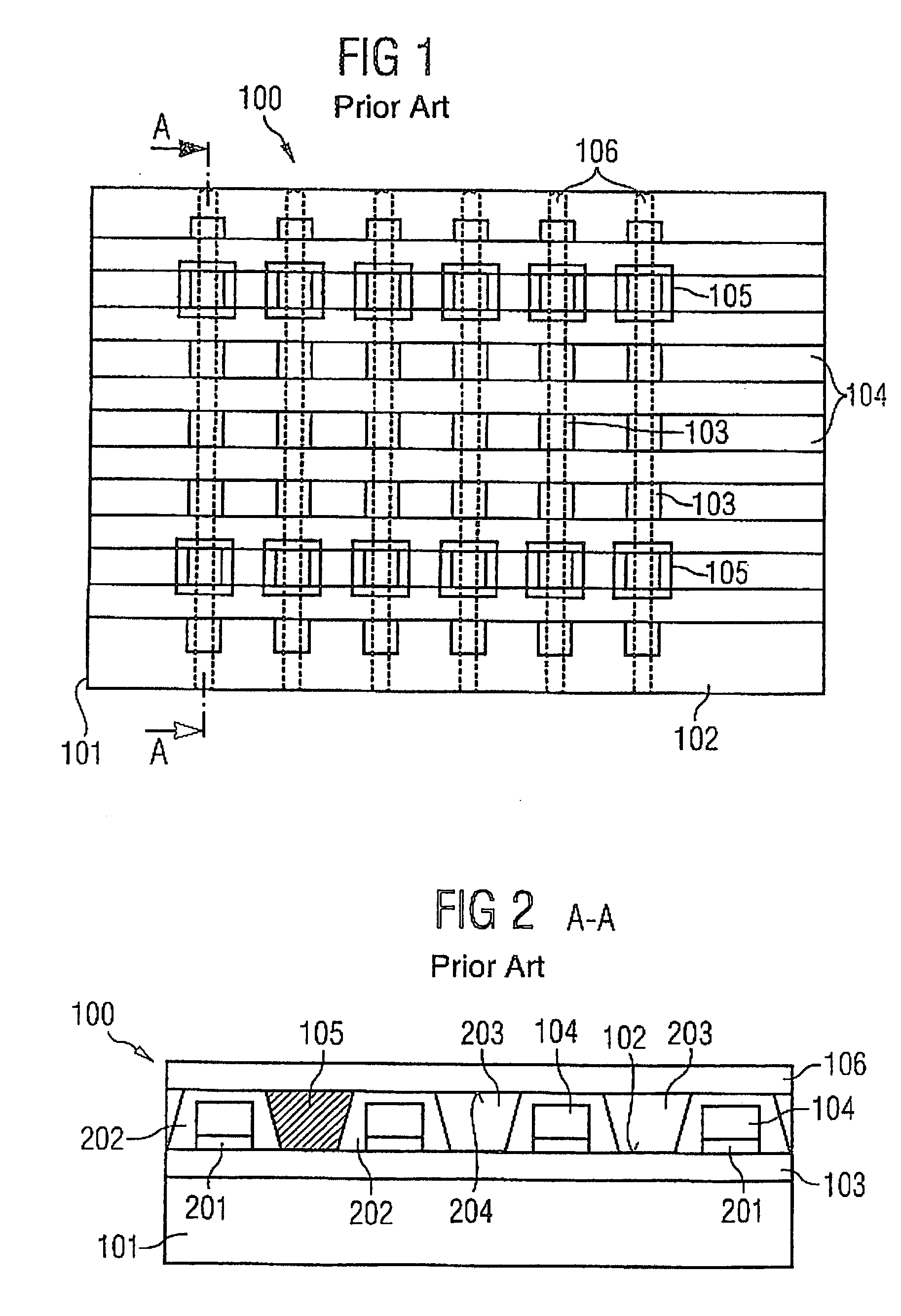
However, diffused-in bit lines have the problem that the electrical resistances of the diffused-in bit lines are higher than the electrical resistances of track conductors in metallization levels.
The RC time constant which results from the level of the resistances of the diffused-in bit lines consequently limits the signal propagation time.
However, the above-described method for producing the self-aligning contacts does not allow alignment parallel to the second track conductors.
Therefore, there is a risk of a contact being produced offset parallel to the second track conductors.
An offset contact of this type can lead to electrostatic effects on the semiconductor substrate, which can cause a short circuit between adjacent diffused-in bit lines.
A short circuit of this type inevitably leads to failure of the immediately adjacent transistors.
It is possible that all the transistors in the relevant bit lines may even be affected by this disturbance.
Therefore, when the etching mask is being produced during the production process for each individual contact, the etching mask has to be positioned very accurately, which involves a high level of outlay.

Method used


Image

  • Method for generating an electrical contact with buried track conductors
  • Method for generating an electrical contact with buried track conductors
  • Method for generating an electrical contact with buried track conductors

Examples


Embodiment Construction

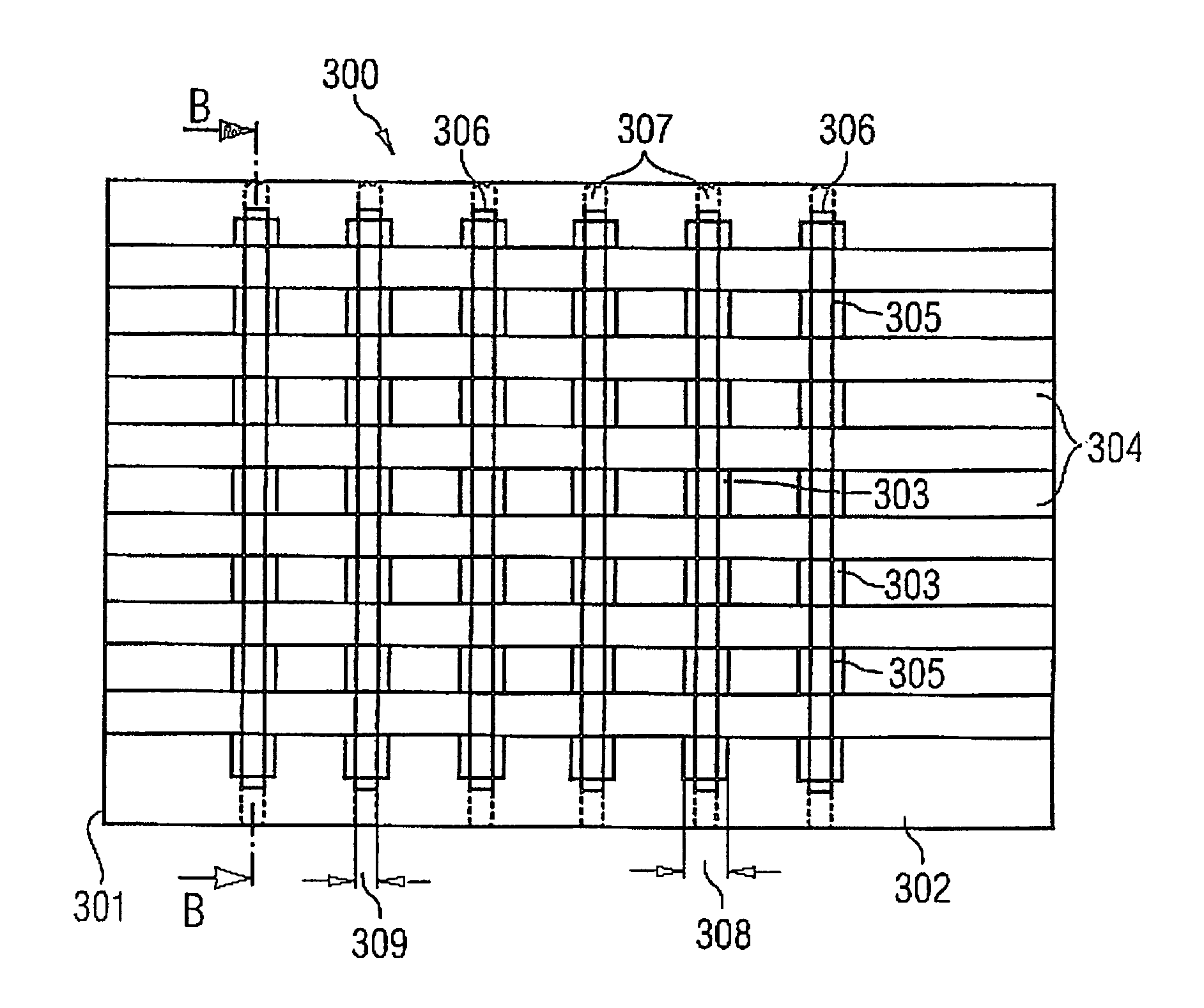
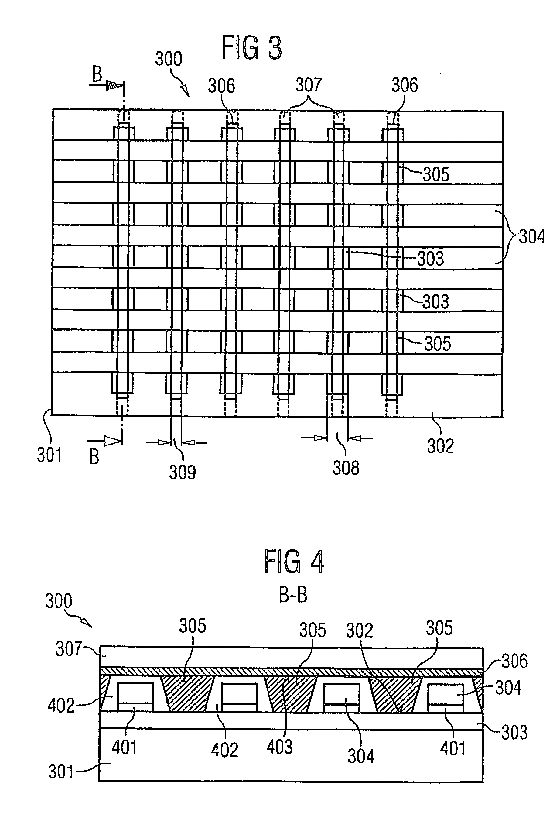
[0044] In the first exemplary embodiment of the invention, a group of first track conductors 303 is integrated in a semiconductor substrate 301 at a substrate surface 302. The first track conductors 303 are arranged substantially parallel to one another and end substantially flush with the substrate surface 302. The first track conductors 303 are usually produced by means of diffusion of electrically conductive ions into the semiconductor substrate 301. The first track conductors 303 may be provided, for example, as buried bit lines.

[0045] Furthermore, a group of second track conductors 304, which are arranged on the substrate surface 302, substantially parallel to one another and electrically insulated with respect to the first track conductors 303, is located on the substrate surface 302 of the semiconductor substrate 301. The second track conductors 304 form a substantially regular grid together with the first track conductors 303. The second track conductors 304 are usually pro...


PUM


Abstract

A semiconductor structure 300 comprises a plurality of first track conductors 303, a plurality of second track conductors 304, which are insulated with respect to the first track conductors 303 and form a grid together with these first track conductors 303, and a plurality of third track conductors 307 parallel above the first track conductors 303, which third track conductors 307 partly cover the second track conductors 304 and are insulated with respect thereto, in which semiconductor structure 300, between in each case two adjacent second track conductors 304, there is located an electrical contact 305 between each first track conductor 303 and the corresponding third track conductor 307 which lies above it.

Description

BACKGROUND OF THE INVENTION [0001] This application is a divisional of U.S. patent application Ser. No. 10 / 159,859, filed May 31, 2002, which claims priority to German Patent Application Number 101 27 350.9, filed Jun. 6, 2001. [0002] The invention relates to a semiconductor structure having buried track conductors and to a method for generating an electrical contact with buried track conductors. [0003] According to the prior art, memory cell arrangements, for example flash memories, are produced as large matrix-like memory arrays comprising transistors. A certain arrangement of track conductors is required both for storage and to read out the memory cells. To optimize the space required, some of the track conductors are diffused into a semiconductor substrate as buried bit lines. However, diffused-in bit lines have the problem that the electrical resistances of the diffused-in bit lines are higher than the electrical resistances of track conductors in metallization levels. [0004] T...

Claims


Application Information

Patent Timeline
Patent Type & Authority Applications(United States)
IPC IPC(8): H01L21/60H01L23/522H01L23/528H01L27/02H10B12/00H10B69/00H10B99/00
CPCH01L21/76897H01L23/522H01L23/528H01L27/115H01L27/10885H01L27/10888H01L27/0207H01L2924/0002H10B12/485H10B12/482H10B69/00H01L2924/00
Inventor LUDWIG, CHRISTOPHMORHARD, KLAUS-DIETERKUTTER, CHRISTOPH
Owner INFINEON TECH AG
Learn More