High-speed TO-can optoelectronic packages

a technology of optoelectronic packages and tocans, applied in the direction of lasers, semiconductor lasers, solid-state devices, etc., can solve the problems of increasing the difficulty of high-speed tasks, package limitations for high-speed applications, and the inability to meet the requirements of high-speed tocan packages, etc., and achieve cost-effective effects

Inactive Publication Date: 2005-09-15
RIAZIAT MAJID LEONARD +2
View PDF4 Cites 23 Cited by
  • Summary
  • Abstract
  • Description
  • Claims
  • Application Information

AI Technical Summary

Benefits of technology

[0007] It is an object of the invention to provide high-speed TO-can packaging for semiconductor lasers, transmitters, receivers, and other optoelectronic components. The cost-effective improvements described herein may further promote the continued success of TO-can packaging in the marketplace as a desirable choice for current high-speed applications demanding data rates of 10 Gbps and greater.

Problems solved by technology

The TO-can package however was not originally designed for relatively high Gbps speeds.
High-speed optoelectronic devices have primarily relied on other more expensive laser packaging solutions such as butterfly modules.
The parasitic reactance associated with the construction of a TO-can package limited its operation for high-speed applications in the past.
Maintaining the balance between the differential signals is crucial however and this task gets progressively more difficult at higher speeds.
Moreover, TO-can packages generally employ bond wires for connecting various optoelectronic components and posts which may further contribute to the undesirable parasitic effects often associated with these types of packages at high data rates.
The current lack of adequate solutions for addressing these limitations can not meet the growing demand for high-speed digital communications services which now require optical transmission links to operate at data rates of 10 Gbps and higher.

Method used


Image

  • High-speed TO-can optoelectronic packages
  • High-speed TO-can optoelectronic packages
  • High-speed TO-can optoelectronic packages

Examples


Embodiment Construction

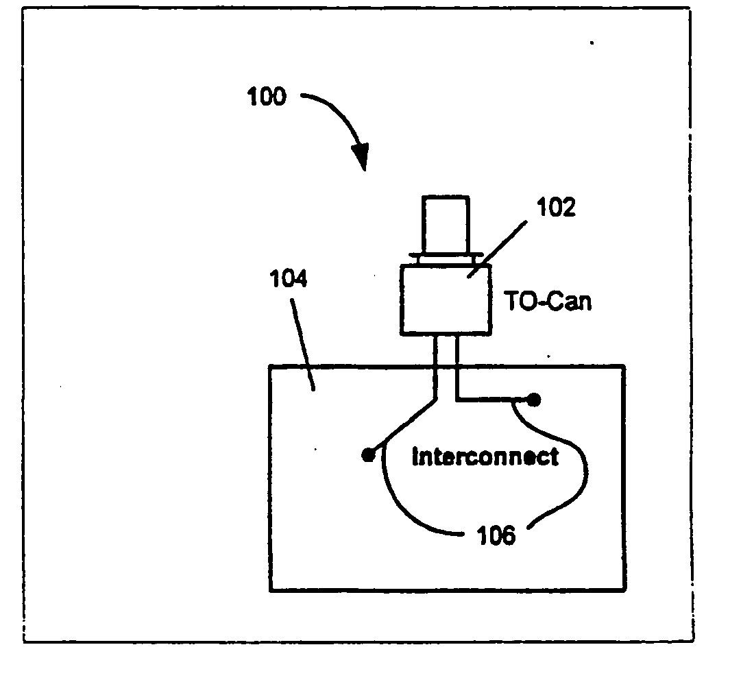
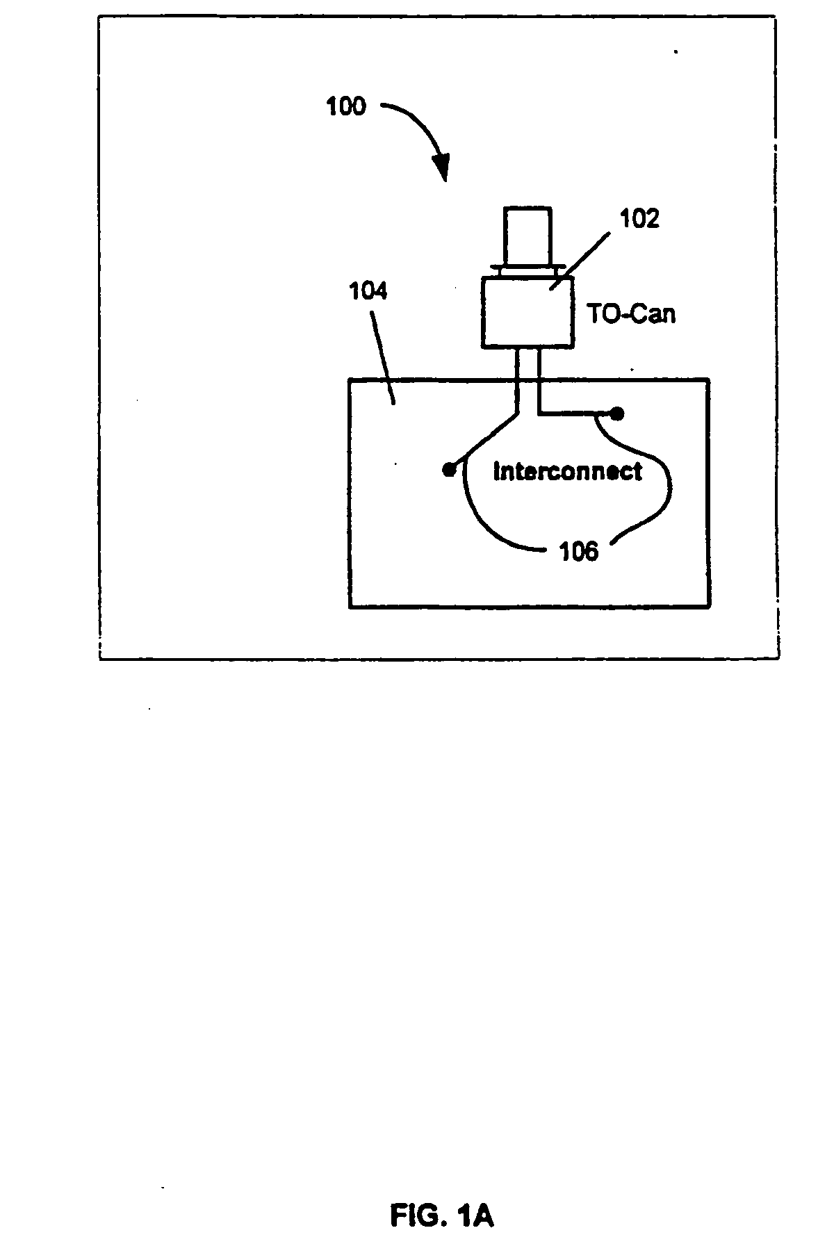
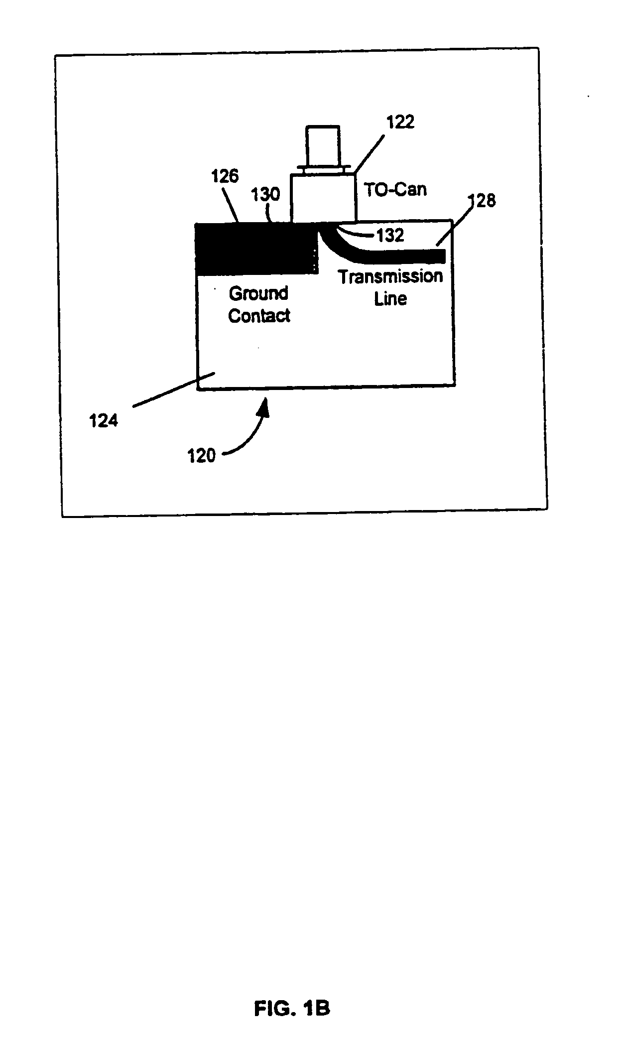
[0037]FIG. 1 (a) illustrates the conventional placement and assembly 100 of a TO-can package 102 on a PC board 104. The TO-can package 102 may be coupled to multiple interconnects 106 for communication with the board. The TO-can package 102 basically comprises a header base and a cap or cover structure that is formed with a window through which light passes. The window may be formed with a lens or other optical element. The TO-can type package 102 provides an enclosure that serves to protect VCSEL components and other contents such as photodetectors or photodiode monitors. The TO-can laser package may include a ground post and one or more signal lines for connection to the PC board 104. Portions of the signal lines may be metallized and formed directly on the board. A top view illustration of the interior region of the TO-can 140 is also provided in FIG. 1(c). The package base may be connected to a ground post for the package and a plurality of signal lines or posts. The TO-can 140 ...


PUM


Abstract

Methods and apparatus that provide TO-can optoelectronic packages suitable for optical telecommunications applications involving data speed rates of up to 10 Gbps and beyond. A TO-can optoelectronic package may comprise a TO-can cap and a TO-can header defining an interior region of the package. An optoelectronic component such as a laser or photodetector can be mounted within the interior region of the TO-can. An electrical connection may be selected for coupling the optoelectronic component to a selected post of the TO-can package. The electrical connection may include a transmission line formed from a conductive element other than a bond wire having a predefined length that can assist in reducing parasitic effects within the TO-can optoelectronic package to accommodate high-speed data rates. The transmission line itself is connected to the optoelectronic component and the selected post with a plurality of bond wires.

Description

CROSS-REFERENCE [0001] This is a continuation application which claims priority under 35 USC § 120 to U.S. patent application Ser. No. 10 / 212,011 filed on Aug. 2, 2002, which claims the benefit of priority to U.S. Provisional Application No. 60 / 350,610 filed on Jan. 18, 2002, which are incorporated herein by reference in their entirety.BACKGROUND OF THE INVENTION [0002] The present invention pertains to semiconductor laser packages, transmitters, and receivers, and more particularly to the packaging of a plurality of optoelectronic components within TO-can package configurations. [0003] Lasers are used for many purposes particularly in the telecommunications industry. Edge emitting lasers are the most common. They are available for all major telecommunication wavelengths and multiple types are available for various applications. Vertical cavity surface emitting lasers (VCSELs) generally offer a low-cost alternative and are capable of being fabricated in larger volumes on semiconduct...

Claims


Application Information

Patent Timeline
Patent Type & Authority Applications(United States)
IPC IPC(8): H01L31/02H01S5/022H01S5/042H01S5/062H01S5/183
CPCH01S5/02212H01S5/02276H01S5/06226H01S5/0683H01S5/183H01L2224/48091H01L2924/30107H01L2924/3011H01L2924/00014H01L2924/00H01S5/02345
Inventor RIAZIAT, MAJID LEONARDTZUANG, CHING-KUNGPAO, YI-CHING
Owner RIAZIAT MAJID LEONARD
Why Eureka
Try Eureka