Method for testing semiconductor integrated circuit

a technology of integrated circuits and semiconductors, applied in the direction of measurement devices, error detection/correction, instruments, etc., can solve the problems of increasing the number of semiconductor-integrated-circuit design process steps, process tends to require more test patterns, and the actual input/output operation of the memory cannot be tested using the paths used during the actual operation, so as to simplify the logic of the memory circuit, reduce the time required for test pattern generation, and reduce the cost of the semiconductor integrated circui

Inactive Publication Date: 2005-09-15
PANASONIC CORP
View PDF4 Cites 23 Cited by
  • Summary
  • Abstract
  • Description
  • Claims
  • Application Information

AI Technical Summary

Benefits of technology

[0052] In the inventive test method, the memory circuit is initialized before a BIST test or a scan test, and the memory circuit is modeled into a combinational sequential circuit in the semiconductor integrated circuit in which no write is performed during the BIST test or scan test. This simplifies the logic of the memory circuit, while allowing the time required for test pattern generation to be reduced.
[0053] Also, if generation of a write operation pattern is prohibited in test pattern generation, it is not necessary to incorporate a write inhibit circuit for inhibiting a write to the memory during a BIST test or a scan test, thereby enabling the costs of the semiconductor integrated circuit to be reduced.
[0054] If the clock applied to the memory circuit is a delay clock which is delayed behind the clock applied to the logic circuits that are forward- and backward-connected to the memory circuit, the memory circuit can be modeled into a combinational circuit and it is possible to generate a test pattern with a conventional full scan test technique. Moreover, in the case of a latest scan test tool, it is also possible to reduce the time necessary for test pattern generation.

Problems solved by technology

Thus, this process tends to require more test patterns.
Therefore, while the memory BIST is being performed, the test pattern is applied to the memory and the output signal is captured from the memory through the paths that are different from the paths used during normal operation, which means that the actual input / output operation of the memory cannot be tested using the paths used during the actual operation.
In these cases, however, the normal operation test pattern is prepared manually, such that a problem arises in that the number of semiconductor-integrated-circuit design process steps increases.
Furthermore, if combinational circuits present between the memory and the storage elements become more complicated, it actually becomes difficult to design the normal operation test pattern.
Moreover, since the verification using logic BIST or scan test and the verification using the normal operation test pattern are performed with separate EDA tools, the process of calculating fault coverage, which indicates how perfect the test is, becomes complicated.
Consequently, it is not possible to test whether the write operation and the read operation to and from the memory are performed properly.
Thus, the establishment of the values for the memory, which can be done in one cycle in actual operation, takes a considerable amount of time.
In a case where no bypass circuits are prepared, all of the memory regions need to be initialized during logic BIST, so this case is actually impossible.

Method used


Image

  • Method for testing semiconductor integrated circuit
  • Method for testing semiconductor integrated circuit
  • Method for testing semiconductor integrated circuit

Examples


first embodiment

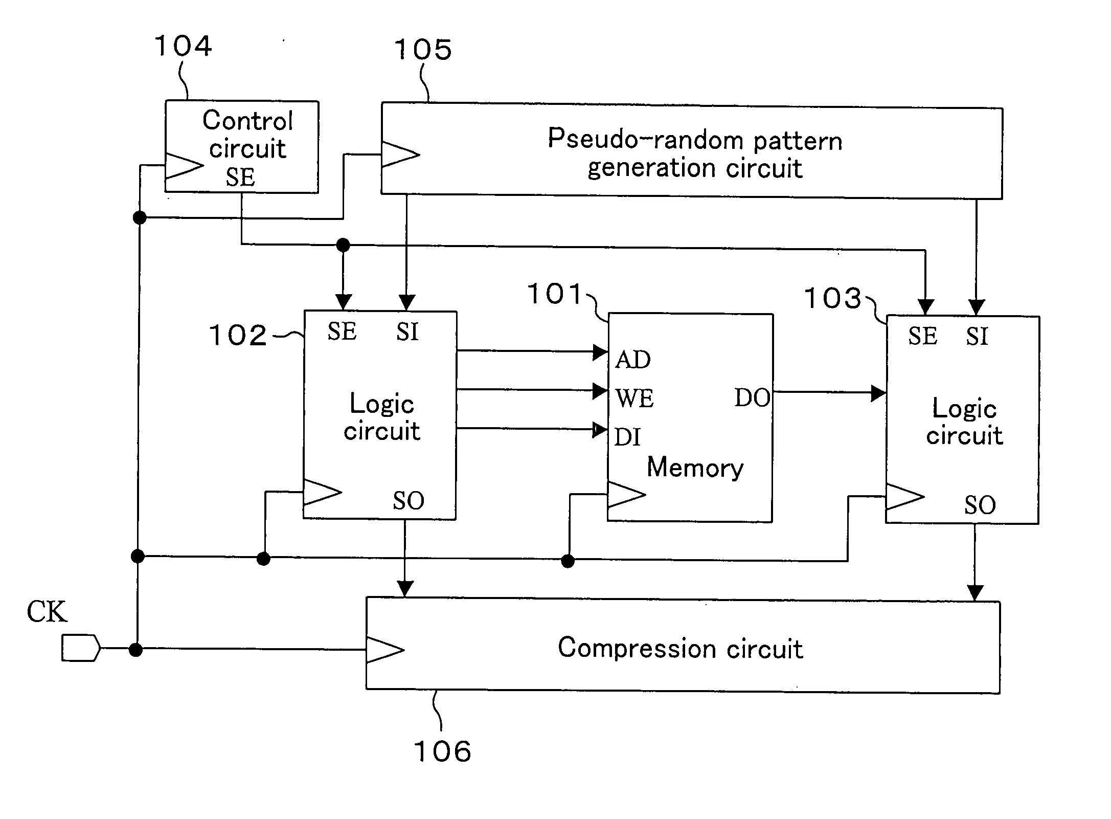
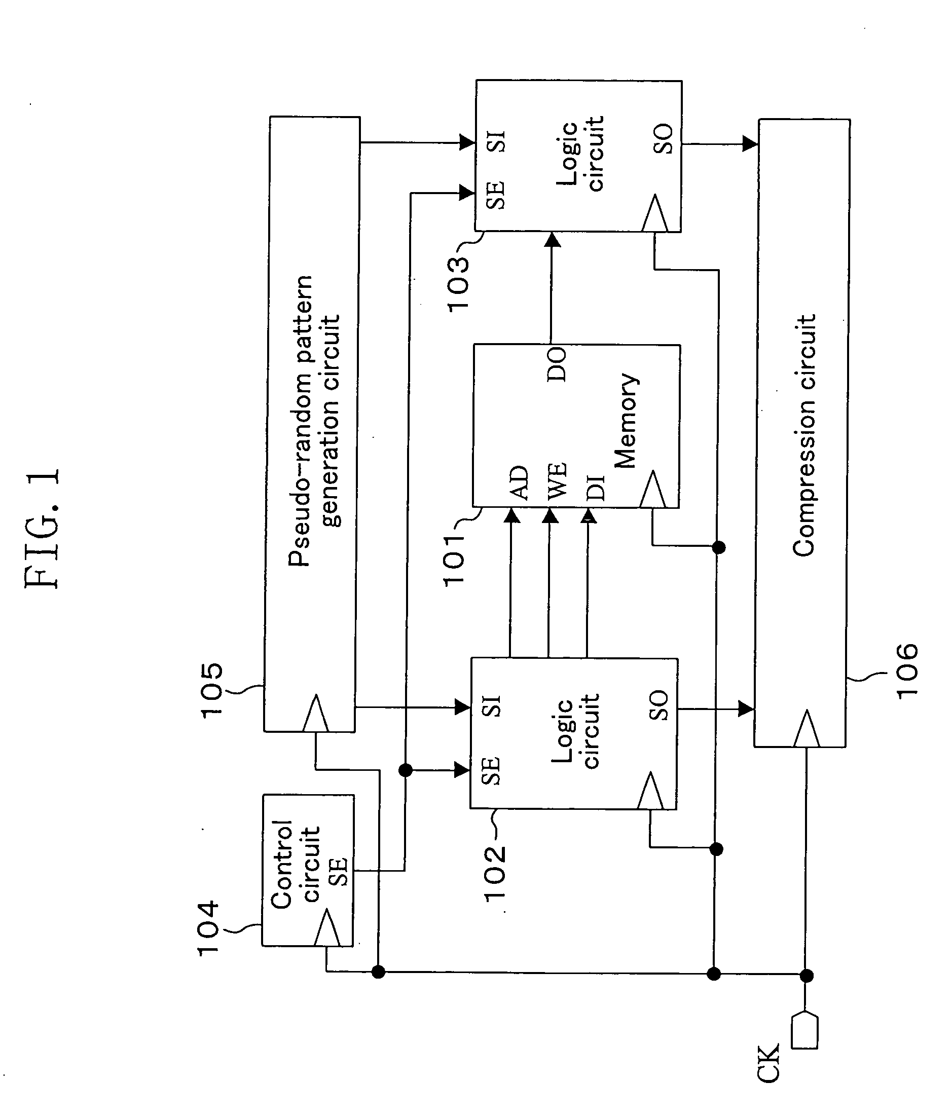
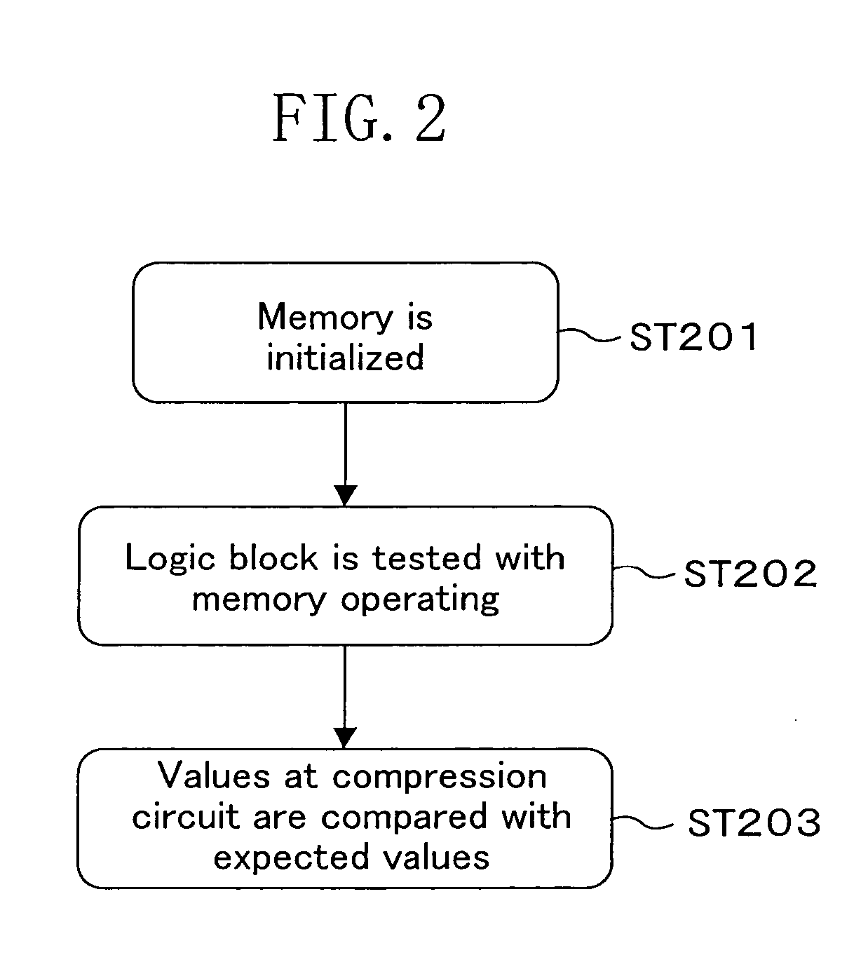
[0069]FIG. 1 is an exemplary semiconductor integrated circuit according to a first embodiment of the present invention. In the first embodiment, at-speed test of the interface (input and output) of a memory 101 included in the semiconductor integrated circuit shown in FIG. 1 will be discussed. The memory 101 is controlled from a logic circuit 102 and an output from the memory 101 is captured into a logic circuit 103. Each of the logic circuits 102 and 103 is of a scan test design and includes scan flip-flops and a combinational circuit portion, with the scan flip-flops forming a scan chain and including scan-in terminals SI, scan-out terminals SO, and scan-enable terminals SE. A pseudo-random pattern generation circuit 105 applies a pseudo-random pattern to the SI terminals of the logic circuits 102 and 103. A compression circuit 106 captures, from the SO terminals, output responses produced from the logic circuits 102 and 103 in reply to the pseudo-random pattern, and then compress...

second embodiment

[0090]FIG. 6 illustrates an exemplary semiconductor integrated circuit according to a second embodiment of the present invention. In the second embodiment, at-speed test of the interface (input and output) of a memory 101 included in the semiconductor integrated circuit shown in FIG. 6 will be discussed.

[0091] In FIG. 6, the memory 101 is controlled from a logic circuit 102 and an output from the memory 101 is captured into a logic circuit 103 by way of a combinational circuit 601.

[0092] A clock signal CK serves as a clock signal for the memory 101 and other blocks. As a clock for the memory 101, a clock that is delayed behind a clock for the logic circuits 102 and 103 by a delay circuit 602 is input.

[0093] A scan-enable signal SE is applied to a SE terminal 603 from an external device. The scan-enable signal SE applied to the SE terminal 603 is supplied to the logic circuits 102 and 103. When the value of the scan-enable signal SE is “1”, a shift operation is performed, by which...


PUM


Abstract

An inventive method is a method for testing a semiconductor integrated circuit that includes a memory circuit provided between a first storage element and a second storage element. The inventive method includes the steps of: (a) initializing the memory circuit; (b) supplying a test pattern to the first storage element; (c) supplying a memory access signal, which corresponds to the test pattern supplied to the first storage element, to the memory circuit through a path that is used in normal operation; (d) capturing a value output from the memory circuit in response to the memory access signal, into the second storage element through a path that is used in normal operation; and (e) comparing the value captured into the second storage element with an expected value.

Description

CROSS-REFERENCE TO RELATED APPLICATION [0001] This application claims priority under 35 U.S.C. § 119 on Patent Application Nos. 2004-13535 filed in Japan on Jan. 21, 2004, and No. 2005-8210 filed in Japan on Jan. 14, 2005, the entire contents of which are hereby incorporated by reference. BACKGROUND OF THE INVENTION [0002] The present invention relates to methods for testing actual operation of a memory interface (input terminal / output terminal). [0003] An operation test of a semiconductor integrated circuit having a memory and logic circuits generally includes two tests: a test of the logic circuits and a test of the memory. Typical tests of a logic circuit are logic BIST and scan test, while typical tests of a memory are memory BIST and memory test performed using a tester. In a test of a logic circuit, wiring or transistors are inspected for defects. On the other hand, in a test of a memory, not only a test similar to the logic circuit test is performed, but relation between valu...

Claims


Application Information

Patent Timeline
Patent Type & Authority Applications(United States)
IPC IPC(8): G06F11/00G11C29/00G01R31/28G11C29/10G11C29/12
CPCG01R31/318547G11C29/36G11C29/12G11C7/20
Inventor MIYAJI, SHINYAICHIKAWA, OSAMU
Owner PANASONIC CORP
Why Eureka
Try Eureka