Design layout preparing method

Active Publication Date: 2005-09-15
KIOXIA CORP
View PDF5 Cites 45 Cited by
  • Summary
  • Abstract
  • Description
  • Claims
  • Application Information

AI Technical Summary

Problems solved by technology

However, the scale-down of the pattern advances; for this reason, it is difficult to faithfully form a pattern in individual processes.
As a result, a problem arises such that the final processed pattern shape is not provided as the design pattern.
With a decrease of the k1 value, a design rule (DR) closely relating with the OPC becomes complicated; for this reason,

Method used


Image

  • Design layout preparing method
  • Design layout preparing method
  • Design layout preparing method

Examples


first embodiment

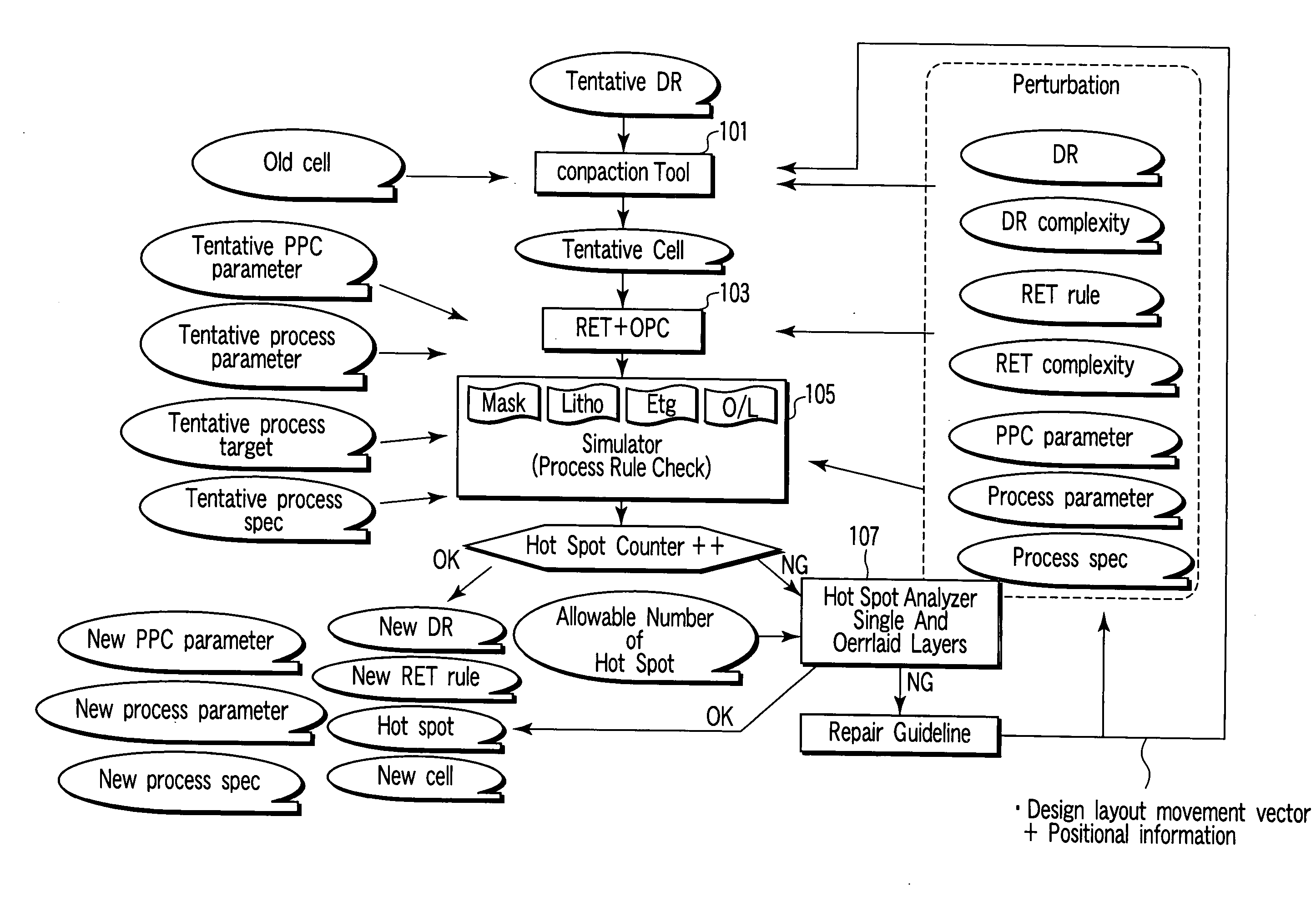
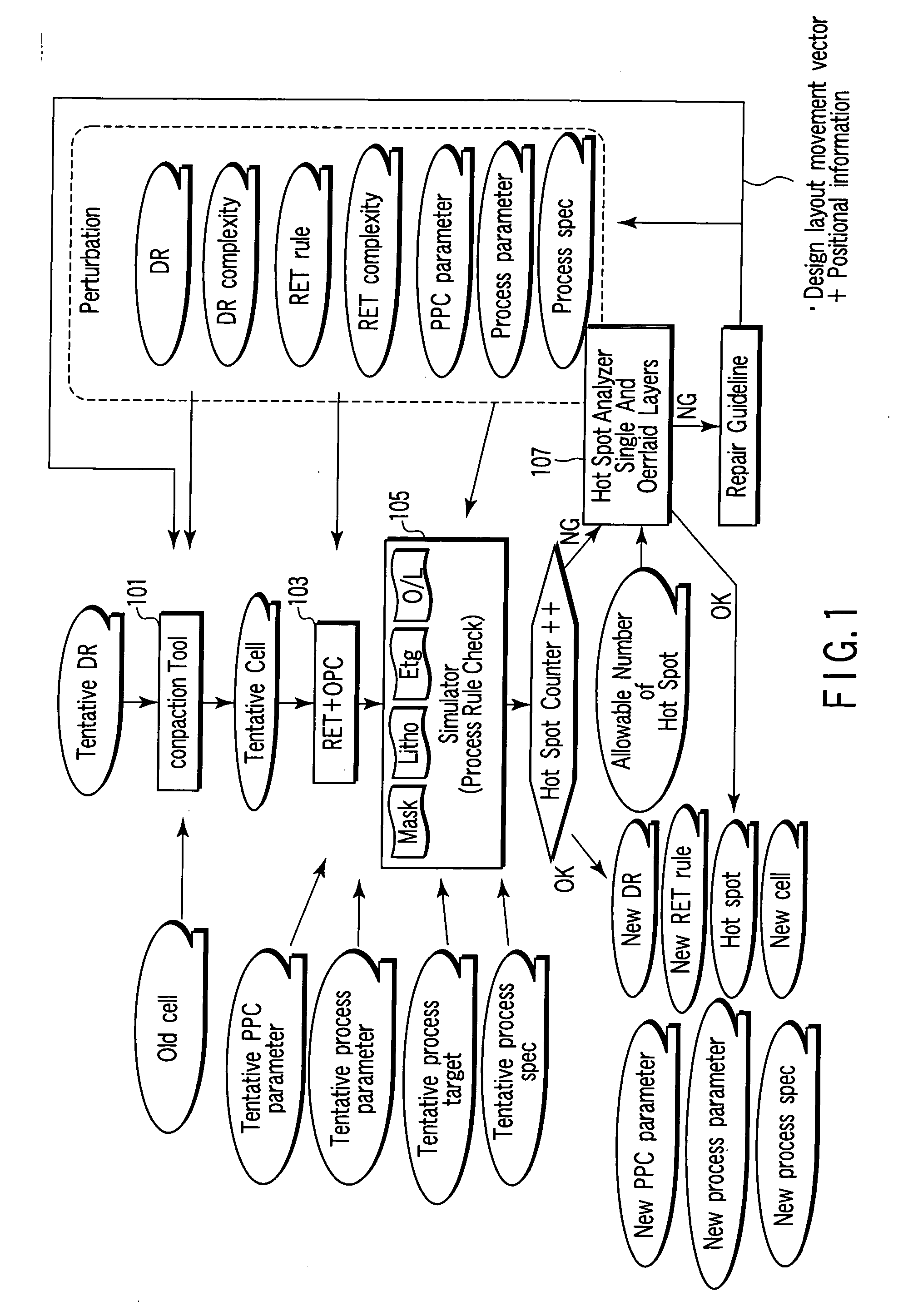
[0028]FIG. 1 is a flowchart to explain the flow of a design layout preparing method according to a first embodiment of the present invention.

[0029] Tentative design rule and layout data are input to a compaction tool 101. In this case, an old-generation standard cell (old cell) is used as layout data. The compaction tool 101 repairs the input layout data so as to satisfy a given design rule (DR). Thus, output layout data (tentative cell) is layout data satisfying the input DR.

[0030] A RET+OPC processing section 103 carries out RET (Resolution Enhancement Technique) processing applied to the foregoing generation with respect to the layout data. The RET processing includes pattern generation processing, pattern delete processing and pattern sort processing. More specifically, the RET processing includes the following processing. One is shifter pasting processing for giving light transmittance and phase to layout data. Another is auxiliary pattern (SRAF: sub-resolution assist feature...

second embodiment

[0065] The pattern repair based on the flow described in the first embodiment was carried out with respect to an actual layout. The following is a description of the results.

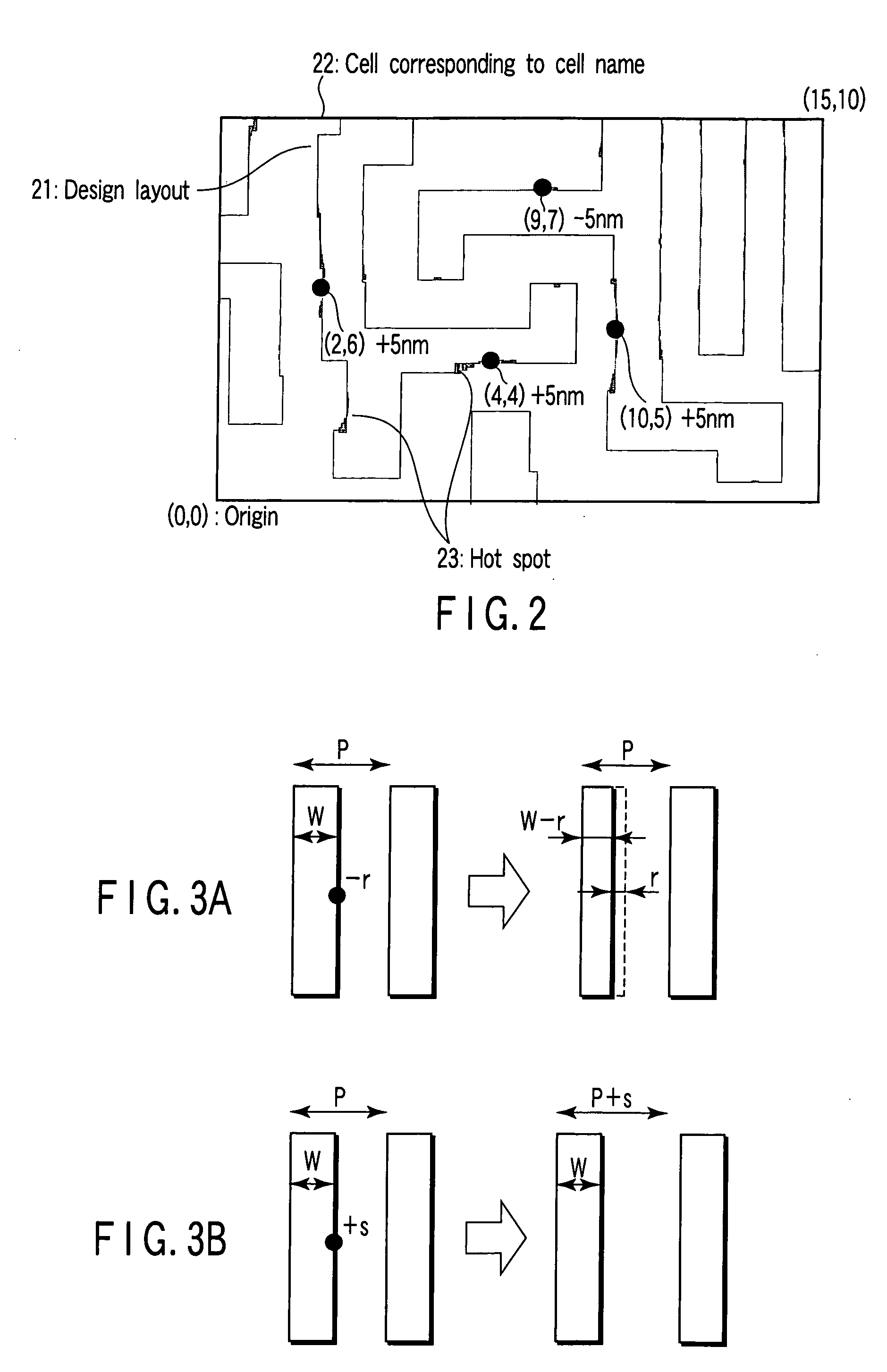
[0066] Under the process condition that the minimum pattern width is 63 nm, and k1=0.3, exposure dose and focus value are varied, and then, a processed pattern shape on a wafer was calculated. More specifically, three (3) conditions are given as the exposure dose, and two (2) conditions were given as the focus. Then, a processed pattern shape was calculated with respect to each of 6 (=3×2) conditions. FIG. 4(a) is a view showing a state that these processed pattern shapes are overlapped. In FIG. 4(a), a hot spot such that an open / short error is predicted appears in portions surrounded by a circle.

[0067] Two values were calculated from the result shown in FIG. 4(a). FIG. 4(b) shows a distribution of the difference (dispersion) between maximum and minimum values of dimension shift generated under the foregoing s...


PUM


Abstract

There is disclosed a method of producing a design layout by optimizing at least one of design rule, process proximity correction parameter and process parameter, including calculating a processed pattern shape based on a design layout and a process parameter, extracting a dangerous spot having an evaluation value with respect to the processed pattern shape, which does not satisfy a predetermined tolerance, generating a repair guideline of the design layout based on a pattern included in the dangerous spot, and repairing that portion of the design layout which corresponds to the dangerous spot based on the repair guideline.

Description

CROSS-REFERENCE TO RELATED APPLICATIONS [0001] This application is based upon and claims the benefit of priority from the prior Japanese Patent Application No. 2003-419601, filed Dec. 17, 2003, the entire contents of which are incorporated herein by reference. BACKGROUND OF THE INVENTION [0002] 1. Field of the Invention [0003] The present invention relates to design layout preparing method and system for preparing a design pattern of a semiconductor integrated circuit. [0004] 2. Description of the Related Art [0005] Recently, the technique of manufacturing semiconductor devices has remarkably advanced, and semiconductor devices having a minimum process dimension of 0.13 μm are mass-produced. The scale-down described above is realized by the great development of micro-pattern forming techniques such as mask-process techniques, photolithography techniques and etching techniques. [0006] In the large pattern size generation, an LSI pattern to be formed on a wafer is intactly used as a d...

Claims


Application Information

Patent Timeline
IPC IPC(8): G03F1/36G03F1/68G03F1/70G06F17/50H01L21/027H01L21/82
CPCH01L21/0271G06F17/5081G06F30/398
Inventor KOTANI, TOSHIYANOJIMA, SHIGEKIKYOH, SUIGENIZUHA, KYOKOOGAWA, RYUJITANAKA, SATOSHIINOUE, SOICHIICHIKAWA, HIROTAKA
Owner KIOXIA CORP
Why Eureka
Try Eureka