Semiconductor chip and display device using the same

a technology of semiconductor chips and display devices, applied in static indicating devices, instruments, optics, etc., can solve the problems of large drawing area of wirings from the terminals around the semiconductor chips, and large limitation of electrode arrangemen

Active Publication Date: 2005-09-22
HANNSTAR DISPLAY CORPORATION
View PDF4 Cites 19 Cited by
  • Summary
  • Abstract
  • Description
  • Claims
  • Application Information

AI Technical Summary

Problems solved by technology

However, in the case of the first conventional technique for reducing the area, although the width of the semiconductor chip can be reduced by providing low-resistance wirings on the semiconductor chip side, drawing area of the wirings from the terminals around the semiconductor chip is large, which only contributes a little for narrowing the frame part.
Therefore, the electrode arrangement may be subject to a large limitation, or there may be a need to add a process of forming an insulating film of a sufficient thickness.

Method used


Image

  • Semiconductor chip and display device using the same
  • Semiconductor chip and display device using the same
  • Semiconductor chip and display device using the same

Examples


first embodiment

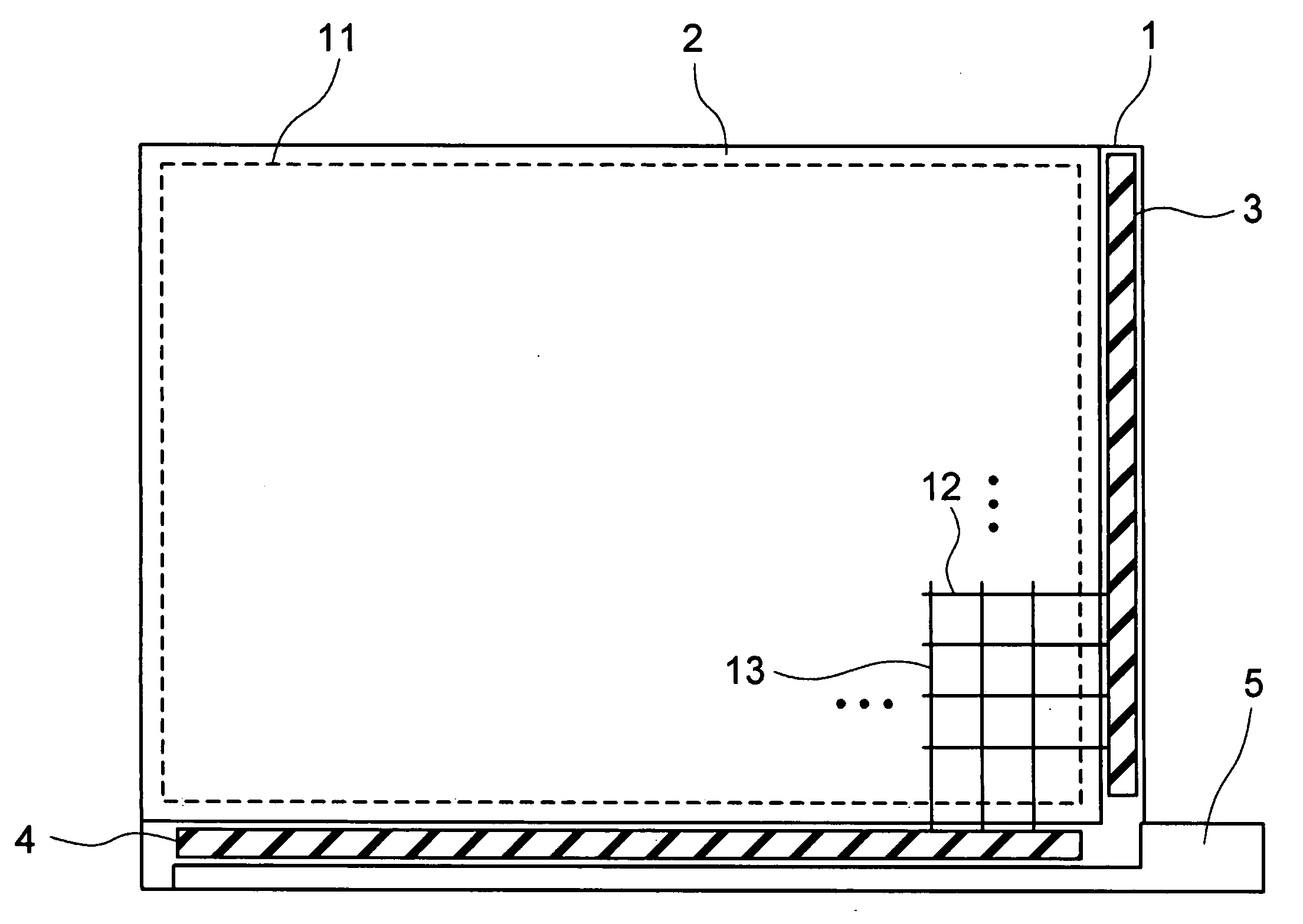
[0045] the present invention will be explained below by way of examples referring to a plan view of a liquid crystal display device shown in FIG. 1 and to the configurations of semiconductor chips shown in FIGS. 2 and 3.

[0046] In the liquid crystal display device shown in FIG. 1, a first substrate 1 and a transparent second substrate 2 are opposed to each other with a liquid crystal layer (not shown) interposed between them, and are bonded together with a sealant. As the first substrate 1 and the transparent second substrate 2, glass substrates are mainly used. Of course, plastic substrates may be used provided that a liquid crystal display device is realized.

[0047] The outer size of the first substrate 1 is larger than that of the transparent second substrate 2. In FIG. 1, the right edge and the lower edge of the first substrate 1 are projected from the second substrate 2, forming a frame part on which semiconductor chips are mounted. On the frame part, semiconductor chips 3 and 4...

sixth embodiment

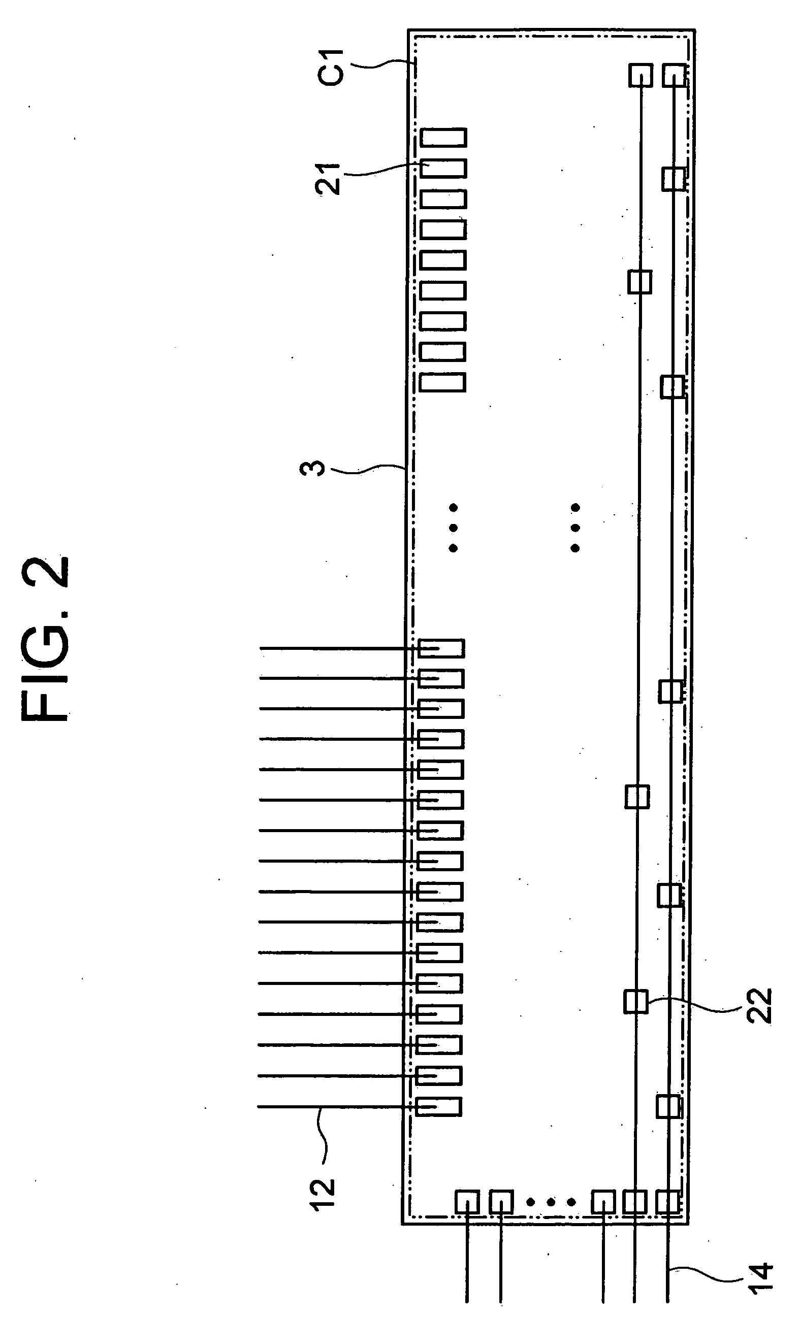
[0103]FIG. 15 is plan view of a liquid crystal display device of the present invention, and FIG. 16 is a plan view of the semiconductor chip 4 for driving signal lines shown in FIG. 15, showing the connecting relationship with the wirings.

[0104] The aspect different from FIG. 13 showing the fifth embodiment is as follows. That is, the flexible wirings 31, corresponding to the control / power supply lines 14, are formed on the flexible wiring board 5B mounted on the frame of the display unit 11. The semiconductor chip 4 is mounted on the flexible wiring board 5B, and the output terminals 21 of the semiconductor chip 4 are connected with the signal lines 13 of the display unit 11, respectively. Further, the connecting terminals 22 of the semiconductor chip 4 are connected with the flexible wirings 31. The connecting terminals 22 arranged on the short edge side of the semiconductor chip 5 are connected with the control / power supply lines 14 formed on the substrate 1. The control / power su...


PUM

PropertyMeasurementUnit
voltageaaaaaaaaaa
lengthaaaaaaaaaa
widthaaaaaaaaaa

Abstract

To realize an area reduction of a semiconductor chip without adding a process, and to provide a semiconductor chip structure having an excellent pressure balance when mounted. In the structure of a semiconductor chip in which control/power supply lines are formed on a glass substrate, connecting terminals for electrically connecting with the control/power supply lines are provided in alignment in the longitudinal direction of the semiconductor device, whereby the wiring length within the semiconductor chip can be suppressed to be minimum. Since the wiring length is shortened, the width of the wirings within the semiconductor chip is narrowed, so that the area of the semiconductor chip is reduced.

Description

BACKGROUND OF THE INVENTION [0001] 1. Field of the Invention [0002] The present invention relates to semiconductor chips having characteristics in the mounting structure and the connecting structure and a display device using the semiconductor chip, and in particular, to reduction of the areas of the semiconductor chips. [0003] 2. Related Art [0004] Recently, display devices using liquid crystal, organic EL (electro-luminescence) or the like are used in various fields such as laptop-computers and mobile phones because of the thin and light characteristics. In order to further reduce the thickness, area and weight, it is required to reduce the area other than the display screen, that is, to narrow the frame part. [0005] A display screen is provided with a display unit, the periphery of which is surrounded by the frame part on which semiconductor chips for driving pixels of the display unit are mounted. These semiconductor chips are mounted on the frame part of the display device by t...

Claims


Application Information

Patent Timeline
Patent Type & Authority Applications(United States)
IPC IPC(8): G02F1/133G02F1/1345G02F1/136G02F1/1362G09G3/36H01L21/3205H01L21/60H01L23/52H01L29/22
CPCG02F1/13454G09G3/3611G09G2300/0426H01L24/06H01L2224/0401H01L2924/01004H01L2224/0603H01L2924/01033H01L2924/01074H01L2924/01082H01L2224/05553H01L2224/05554H01L2924/01006H01L2924/14H01L2924/00
Inventor MIYASAKA, DAIGO
Owner HANNSTAR DISPLAY CORPORATION
Why Eureka
Try Eureka