Liquid crystal display device and its manufacturing method

a technology of liquid crystal display and manufacturing method, which is applied in non-linear optics, instruments, optics, etc., can solve the problems of uneven luminance and spots, and achieve the effect of improving the reliability of long-time/long-term us

Inactive Publication Date: 2005-09-22
SHARP KK
View PDF15 Cites 17 Cited by
  • Summary
  • Abstract
  • Description
  • Claims
  • Application Information

AI Technical Summary

Benefits of technology

[0016] The present invention was made in view of the above situation, and has an object to provide a liquid crystal display device in which unevenness of display, spots, and so forth g

Problems solved by technology

(2) Impurity ions kept by a dummy electrode or a dummy pixel enter a disp

Method used


Image

  • Liquid crystal display device and its manufacturing method
  • Liquid crystal display device and its manufacturing method
  • Liquid crystal display device and its manufacturing method

Examples


embodiment 1

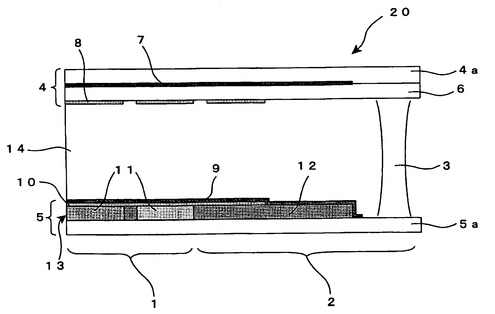
[0096] The liquid crystal display panel 20 illustrated in FIG. 1A and 1B is a panel constituting an active matrix system liquid crystal display device and so forth, and comprises the first substrate 4 and the second substrate 5.

[0097] The first supporting substrate 4a is a transparent substrate such as glass substrate or plastic substrate, and the first substrate 4 has a structure in which the TFT circuitry layer 7 comprising TFT element, source electrode, gate electrode, electrode for storage capacitor and so forth, the insulating layer 6, the picture element electrode 8 and alignment layer (not illustrated) are deposited on the first supporting substrate 4a in this order towards the liquid crystal layer 14. The supporting second substrate 5a is a transparent substrate such as glass substrate or plastic substrate, and the second substrate 5 has a structure in which the color filter layer 13, the transparent electrode 10 and the alignment layer 9 are deposited on the second support...

embodiment 2

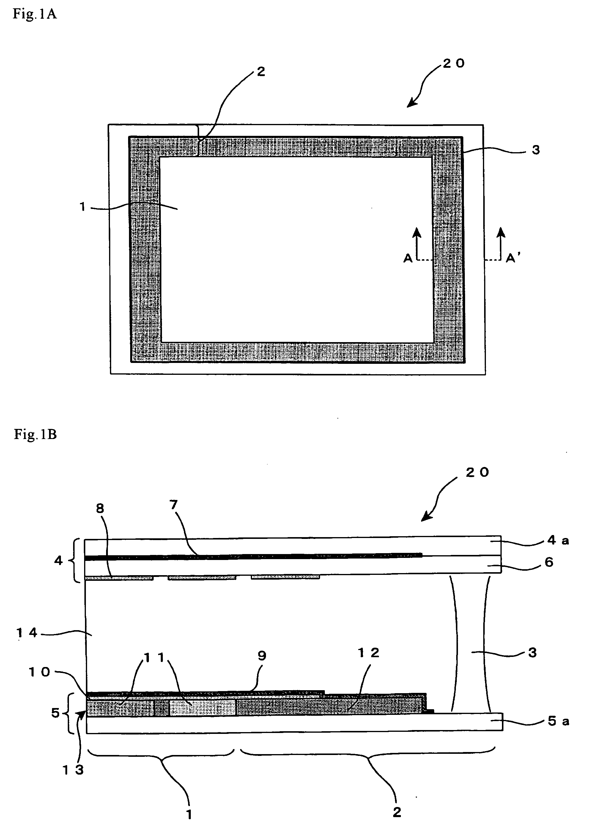
[0108] Each of FIGS. 2A and 2B is a schematic sectional view illustrating structure of the liquid crystal display panel 21 which constitutes a liquid crystal display device according to another embodiment of the present invention. Hereinafter, a description of the same component as the liquid crystal display panel 20 illustrated in FIGS. 1A and 1B will be omitted.

[0109] In the liquid crystal display panel 20 illustrated in FIG. 1B, the seal member 3 is not in contact with the color filter layer 13 in the second substrate 5, but in the liquid crystal display panel 21 illustrated in FIG. 2A, the seal member 3 is in contact with a color filter layer 13 in the second substrate 5. The alignment layer 9, which is formed on the color filter layer 13 in the non-display region 2, is formed until it comes in contact with the seal member 3, and the liquid crystal layer 14 is not directly in contact with the color filter layer 13. It is allowable that the alignment layer 9 is formed until it o...

embodiment 3

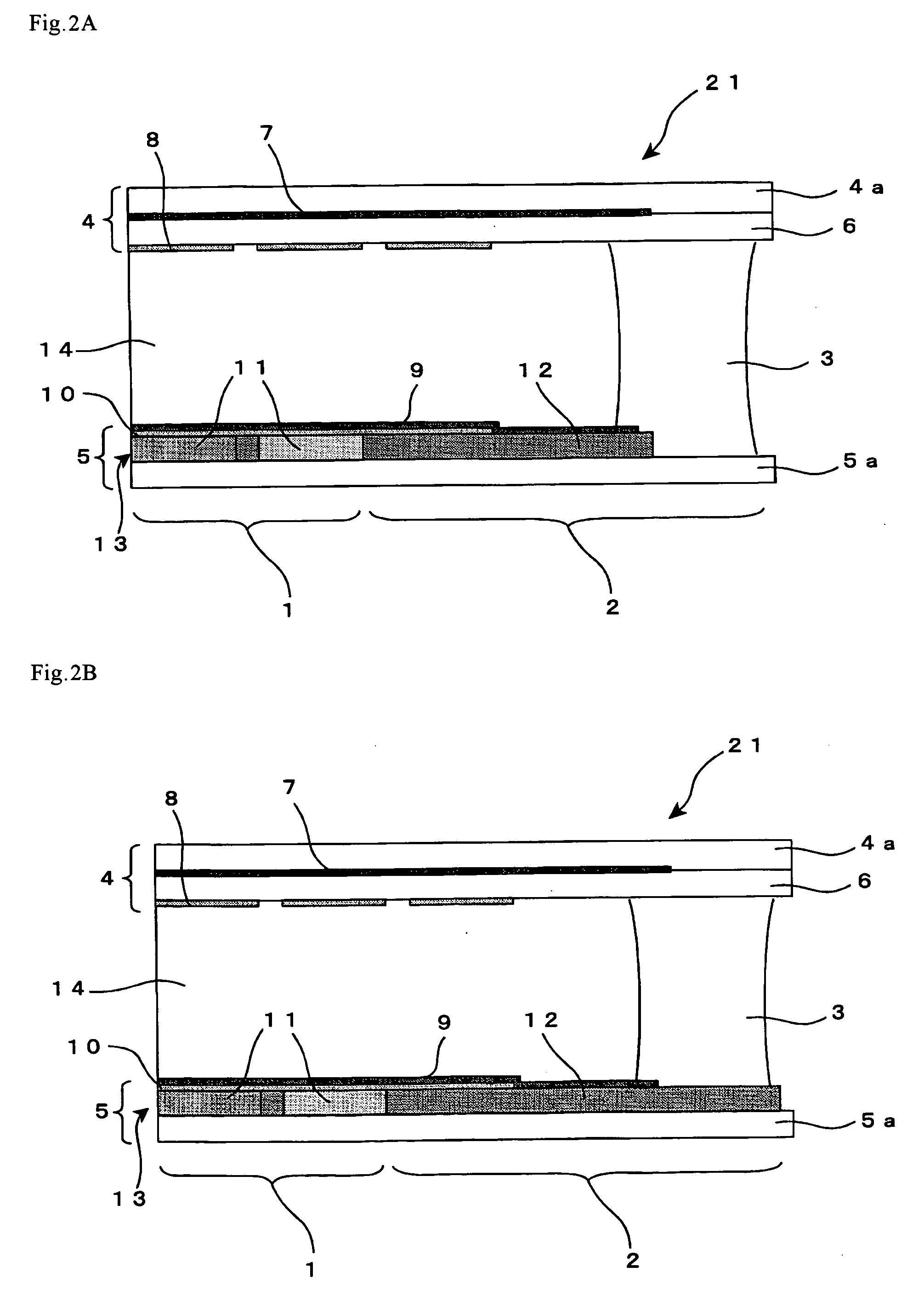
[0114]FIG. 3 is a schematic sectional view illustrating a structure of the liquid crystal display panel 22 according to another embodiment of the present invention. Hereinafter, a description of the same component as liquid crystal display panel 20 illustrated in FIGS. 1A and 1B will be omitted.

[0115] In the liquid crystal display panel 20 illustrated in FIG. 1, the transparent electrode 10 is formed on part of the color filter layer 13 in the non-display region 2, but in the liquid crystal display panel 22 illustrated in FIG. 3, the transparent electrode 10 and the alignment layer 9 are formed at least on the liquid crystal layer 14 side of the color filter layer 13 in the non-display region 2. That is, whole of the color filter layer 13 is covered with the transparent electrode 10, and whole of the transparent electrode 10 is covered with the alignment layer 9. Thus, effect of preventing elution of impurity ions to the liquid crystal layer 14 may be improved by forming the transp...


PUM


Abstract

A liquid crystal display device of the present invention is one in which unevenness of display, spots generated due to lowering of voltage retention because of impurity ions are sufficiently eliminated and reliability of long-time/long-term use is improved. A liquid crystal display device of the present invention is one comprising a first substrate and a second substrate configured via a liquid crystal layer and a seal, wherein at least one of the first substrate and the second substrate comprises, towards the liquid crystal layer, a color filter layer, a transparent electrode and an alignment layer in this order and at least one of the transparent electrode and the alignment layer covers the color filter layer in a non-display region.

Description

REFERENCE TO RELATED APPLICATION [0001] This Nonprovisional application claims priority under 35 U.S.C. § 119(a) on Patent Application No. 2004-074555 filed in Japan on Mar. 16, 2004, the entire contents of which are hereby incorporated by reference. BACKGROUND OF THE INVENTION [0002] 1. Field of the Invention [0003] The present invention relates to a liquid crystal display device and its manufacturing method, and more particularly it relates to an active matrix system liquid crystal display device in which each of picture element electrodes arranged in a matrix form is selectively driven by active element, and its manufacturing method. [0004] 2. Description of the Related Art [0005] Liquid crystal display device is indispensable to a means for displaying information or image, and recently, an active matrix system liquid crystal display device is widely used in applications such as TV and monitor. In such applications, a liquid crystal display device is lighted over a long time and ...

Claims


Application Information

Patent Timeline
IPC IPC(8): G02F1/1335G02F1/1339G02F1/1343
CPCG02F1/133514G02F1/1343G02F1/13394
Inventor HASHIMOTO, YOSHIHIROYAMAGUCHI, HIDEHIKOIWAMOTO, TAKASHIHAYANO, TAKAYUKIYAMADA, NAOSHITSUBATA, TOSHIHIDE
Owner SHARP KK
Why Eureka
Try Eureka