Radiation-emitting semiconductor component

Active Publication Date: 2005-09-22
OSRAM OLED
View PDF18 Cites 11 Cited by
  • Summary
  • Abstract
  • Description
  • Claims
  • Application Information

AI Technical Summary

Benefits of technology

[0019] In a fourth preferred refinement of the invention, the first active zone and the second active zone are formed such that they are electrically drivable separately from one another, with the result that the operating states of the coherent radiation and of the incoherent radiation can be decoupled from one another. The semiconductor component can thus emit radiation having the wavelengths λ1 and/or λ2. This is advantageous if, by way of example, the incoherent radiation is intended to be turned off during operation of the radiation-emitting semiconductor component, for instance in order to avoid disadvantageous influences of this radiation on measurements. Furthermore, a semiconductor component of this type may also be driven in such a way as to emit only incoherent radiation. Coherent radiation can be turned on, after which the component will emit both radiations so that the operating state of the coherent

Problems solved by technology

However, a semiconductor component of this type is not suitable, or is only inadequately suitable, f

Method used


Image

  • Radiation-emitting semiconductor component
  • Radiation-emitting semiconductor component
  • Radiation-emitting semiconductor component

Examples


Example

DETAILED DESCRIPTION OF THE DRAWINGS

[0024] Elements that are of the same kind and act identically are provided with the same reference symbols in the figures.

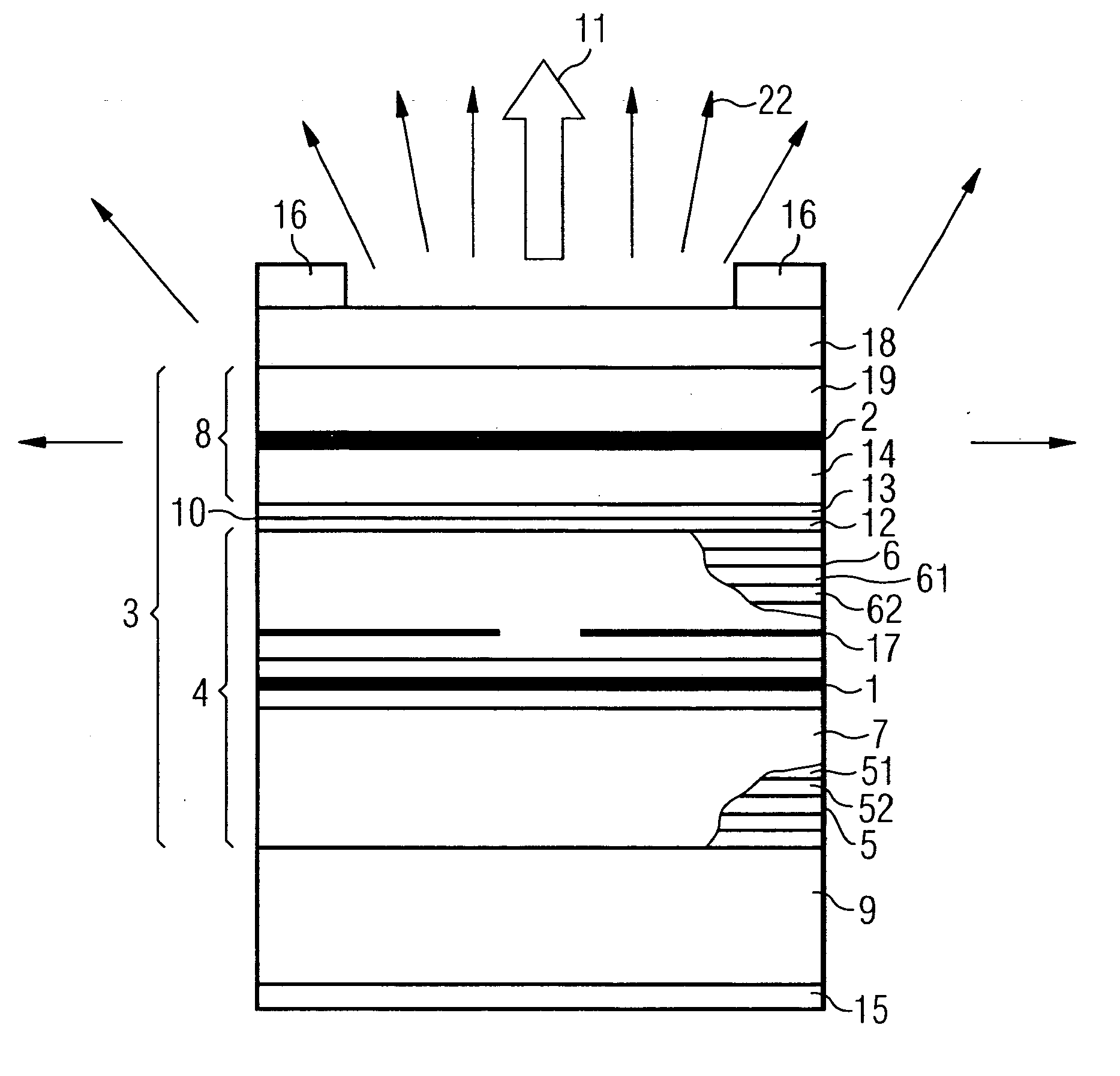
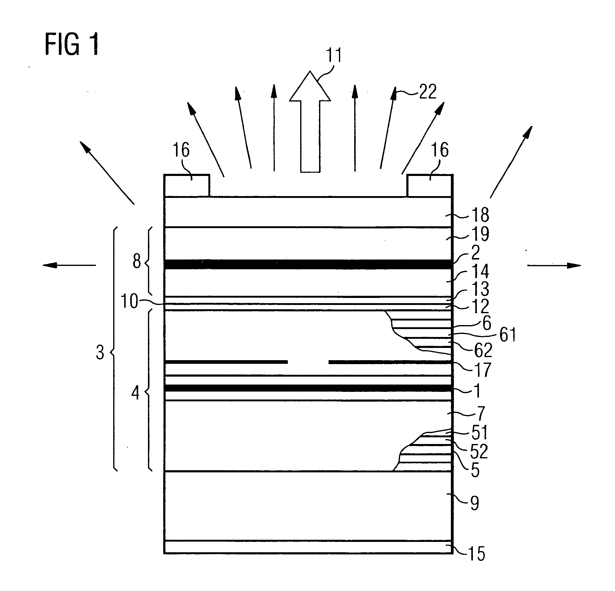
[0025]FIG. 1 illustrates a schematic sectional view of a first exemplary embodiment of a radiation-emitting semiconductor component according to the invention.

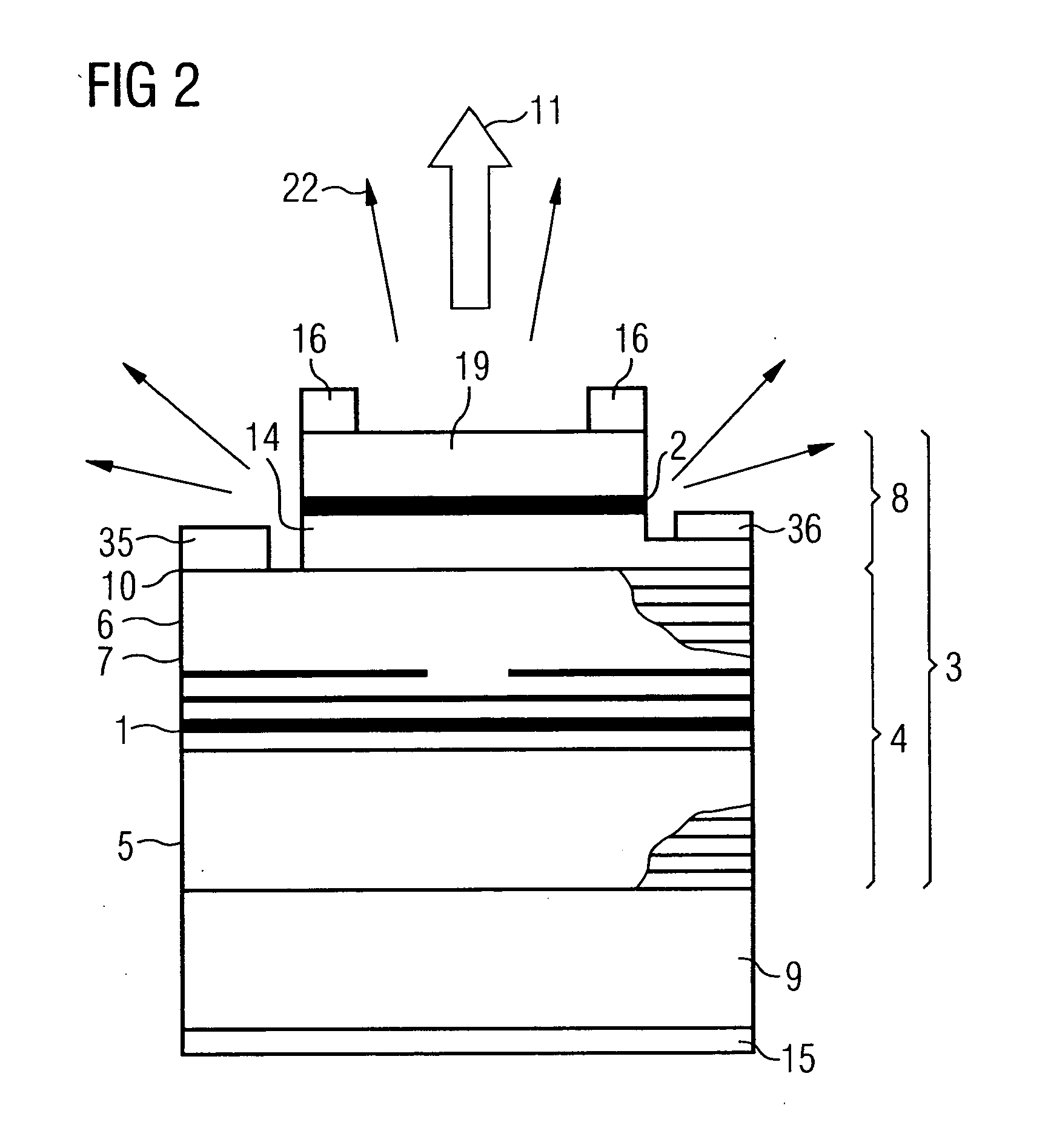
[0026] A semiconductor body 3 comprises a first active zone 1 and a second active zone 2, the first active zone generating coherent radiation 11 having a wavelength λ1 and the second active zone generating incoherent radiation 22 having a wavelength λ2. In this exemplary embodiment, the first active zone 1 is formed in a laser structure 4 corresponding to a VCSEL. A first, preferably n-conducting, mirror 5 and a second, preferably p-conducting, mirror 6, which, by way of example, are in each case formed as Bragg mirrors and have a plurality of schematically illustrated semiconductor layer pairs 51, 52 and 61, 62, respectively, having different refractive indices, form ...


PUM


Abstract

A radiation-emitting semiconductor component comprising a semiconductor body (3) with a first active zone (1) and a second active zone (2) arranged above the first active zone, the first active zone being provided for generating a radiation having a first wavelength λ1 (11) and the second active zone being provided for generating a radiation having a second wavelength λ2 (22), the radiation having the first wavelength λ1 being coherent and the radiation having the second wavelength λ2 being incoherent.

Description

RELATED APPLICATIONS [0001] This patent application claims the priority of German patent application no. 10 2004 004 781.2 dated Jan. 30, 2004, the disclosure content of which is hereby explicitly incorporated by reference into the present description. FIELD OF THE INVENTION [0002] The invention relates to a radiation-emitting semiconductor component BACKGROUND OF THE INVENTION [0003] Radiation-emitting semiconductor components of this type may be embodied for example as in U.S. application Ser. No. 10 / 432,187, as two or more edge emitting lasers arranged one above the other, the respective active zones emitting coherent radiation having the wavelength λ1 and λ2, respectively, during operation. Since the radiation power of coherent radiation having a specific wavelength is essentially emitted only along a main emission direction, an observer observing the radiation-emitting semiconductor component from a direction that deviates from the respective main emission direction of the radi...

Claims


Application Information

Patent Timeline
IPC IPC(8): H01L27/15H01L33/08H01S3/10H01S5/026H01S5/18H01S5/183H01S5/20H01S5/40
CPCH01L27/15H01L33/08H01S2301/18H01S5/0425H01S5/18311H01S5/026H01S5/18386
Inventor PHILIPPENS, MARCALBRECHT, TONY
Owner OSRAM OLED
Why Eureka
Try Eureka