
Chip packaging structure and method of making wafer level packaging

Inactive Publication Date: 2005-09-29
XINTEC INC
View PDF7 Cites 4 Cited by
  • Summary
  • Abstract
  • Description
  • Claims
  • Application Information

AI Technical Summary

Benefits of technology

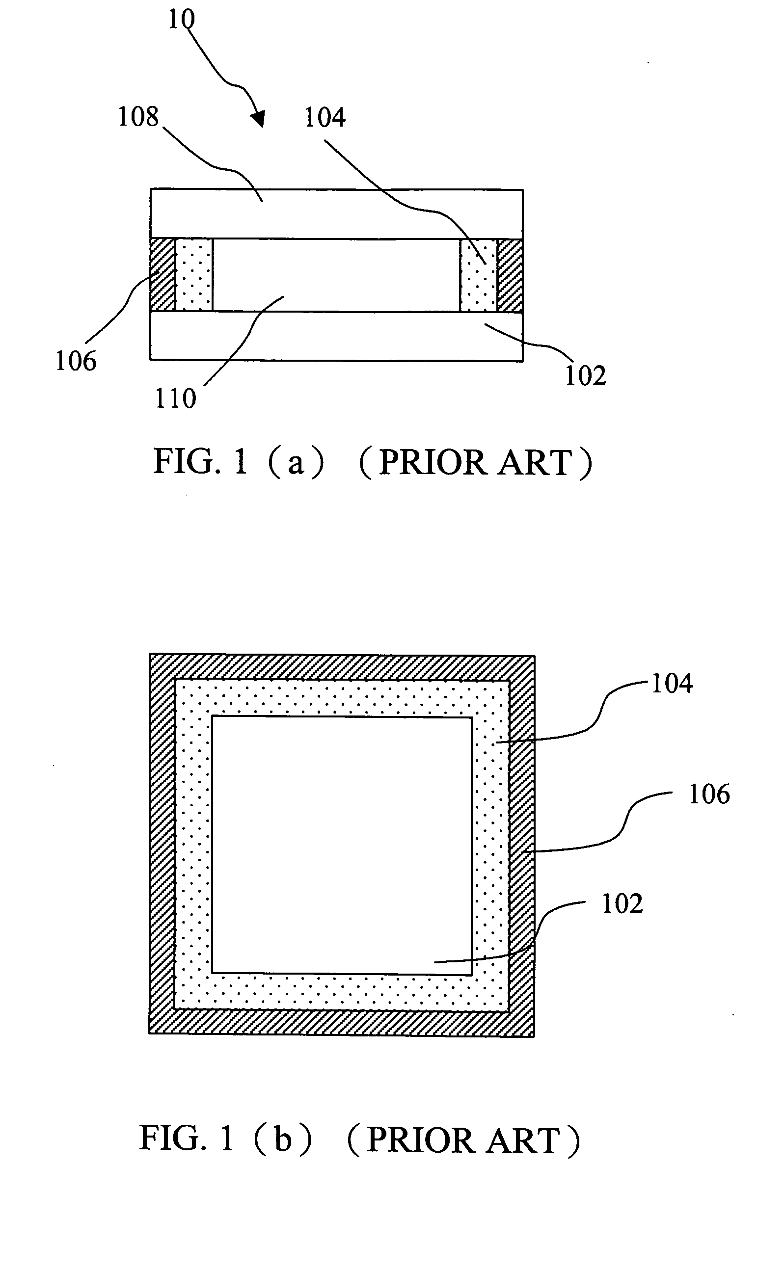
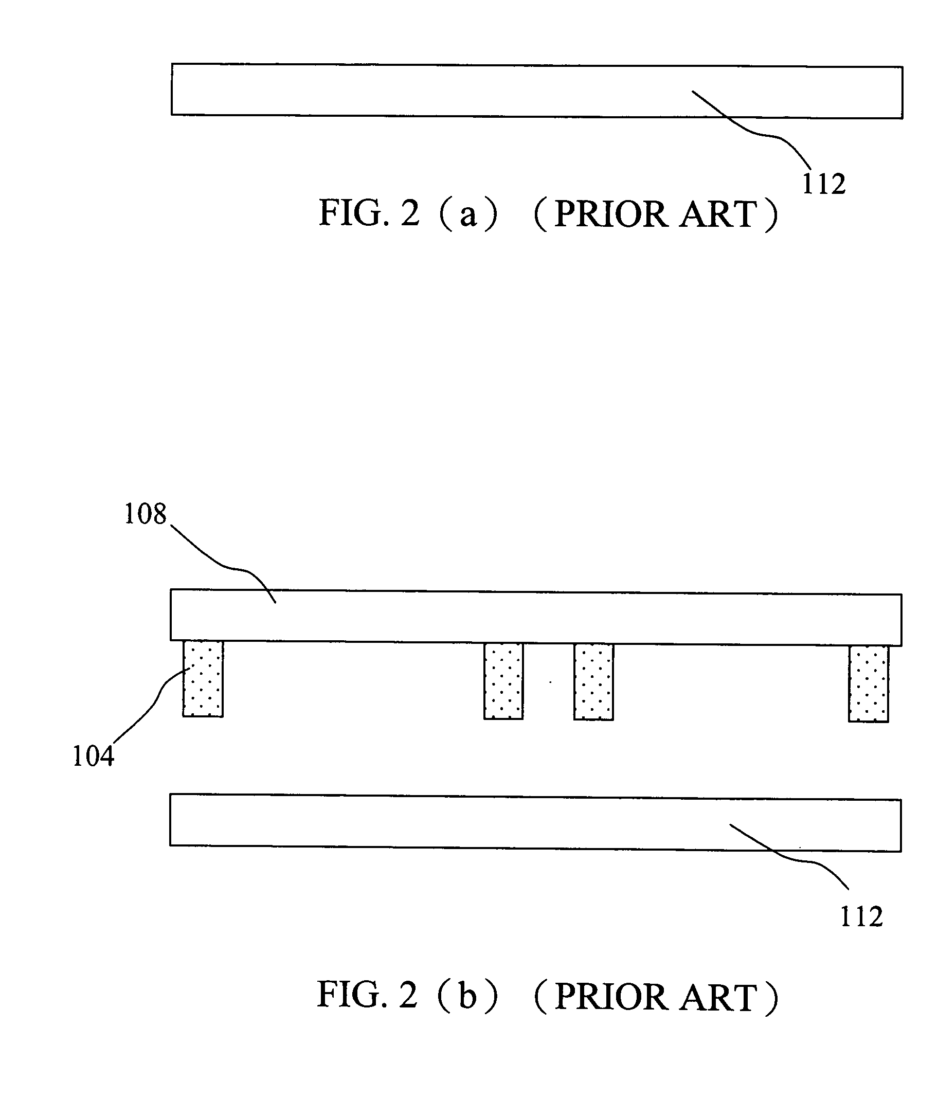
[0008] The primary object of the present invention is to provide a chip packaging structure and method of making wafer level packaging, which improve the disadvantages of prior art, that needs to align. The advantage of the manufacturing process more convenient is achieved.
[0009] Another object of the present invention is to provide a chip packaging structure and method of making wafer level packaging, wherein a transparent is covered over the frame glue under the condition of vacuum, filling the inert gas or in low air pressure environment. It renders chip packaging structure not easy to blow out. Therefore, it has higher reliability.
[0010] Another object of the present invention is to provide a chip packaging structure and method of making wafer level packaging under the condition of vacuum, filling inert gas or low air pressure environment. Due to the refractive index is “1” under vacuum condition, it has huge difference with the refractive index 1.5˜1.6 of lenticular on the chip pattern. It improves the focusing effect of the lenticular and increasing the yield of luminous flux, reliability, and photosensitive.

Problems solved by technology

It renders chip packaging structure not easy to blow out.

Method used


Image

  • Chip packaging structure and method of making wafer level packaging
  • Chip packaging structure and method of making wafer level packaging
  • Chip packaging structure and method of making wafer level packaging

Examples


Embodiment Construction

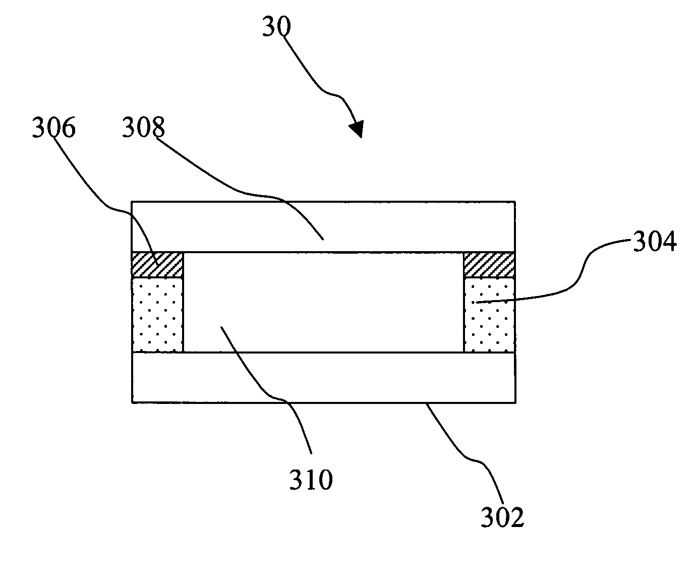
[0020] The cross-sectional view of the present invention as shown in FIG. 3(a), the chip packaging structure 30 comprises a chip 302, a dam 304 surrounding the perimeter of the chips 302, and a frame glue 302 coating on the surface of the dam 304. A transparent cover 308, such as the glass, is covered over the top of the frame glue 306 and adhered against the dam 304 by the frame glue 306. A sealed space 310 is formed between the transparent cover and the chip, wherein the sealed space 310 is in the condition of vacuum, filling the inert gas, such as nitrogen, or low gas pressure environment.

[0021] The present invention also provides a chip packaging structure and method of making wafer level packaging. As shown in FIGS. 4(a) to (d), there are the cross-sectional views showing the steps according to the present invention. First of all, as shown in FIG. 4(a), a wafer 312 is provided, wherein a plurality of chip patterns are formed on the top of the wafer 312. As shown in FIG. 4(b), ...


PUM


Abstract

The present invention provides a chip packaging structure and method of making wafer level packaging. Chip packaging structure comprises a chip, a dam formed surrounding the perimeter of the chip, and a frame glue coated over the surface of the dam. A transparent cover is formed on the top of the frame glue and adhered against the dam by the frame glue. A sealed space is formed between the transparent cover and the chip. The method of making wafer level packaging comprises the steps of: providing a wafer having a plurality of chip patterns thereon; forming a plurality of dams on the wafer and forming each dam surrounding each chip pattern; coating a frame glue over the surface of each dam; covering the transparent cover over the frame glue to form a plurality of sealed spaces between the transparent cover and the wafer, wherein each sealed space comprises a chip pattern; and dicing the chip patterns over the wafer as units in form a plurality of chip packaging structures. The present invention has highly reliability, high yield of luminous flux and photosensitive, simple manufacturing process and adhering frame glue uniformly.

Description

BACKGROUND OF INVENTION [0001] 1. Field of the Invention [0002] The present invention relates to a chip packaging structure and method of making wafer level packaging, and more particularly to a chip packaging structure and method of making wafer level packaging having highly reliability, high yield of luminous flux and photosensitive. [0003] 2. Description of the Prior Art [0004] Semiconductor technologies follow with rapid growing functions of computer and network communication products that essential to meet the requests of diversification, portable, light, thin and minimize. It makes chip packaging industrial away from traditional skills and developing towards high precision with high power, high density, light, thin and minimize, etc. Besides, electronics packaging more over needs high reliability and good cooling characters. Particularly, we must be more carefully with luminous flux, performance of photosensitive and reliability after finishing packaging of optical elements. [...

Claims


Application Information

Patent Timeline
IPC IPC(8): H01L21/44H01L21/50H01L23/10H01L23/12
CPCH01L21/50H01L23/10H01L2924/0002H01L2924/00
Inventor CHAO, DENNYLEE, NICOCHENG, CYRIL
Owner XINTEC INC
Learn More