

Method of manufacturing optical waveguide device
- Summary
- Abstract
- Description
- Claims
- Application Information
AI Technical Summary
Benefits of technology
Problems solved by technology
Method used
Image

Examples
Embodiment Construction
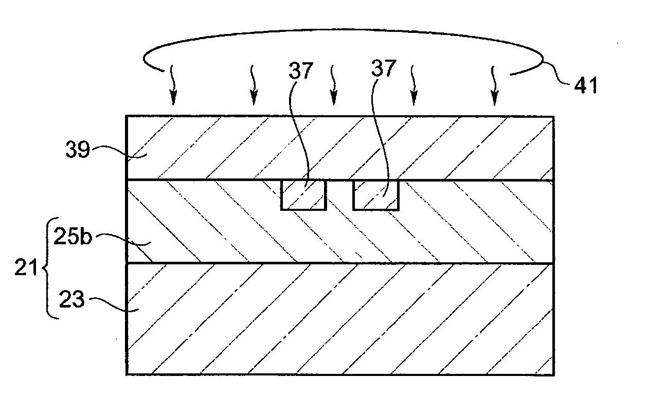
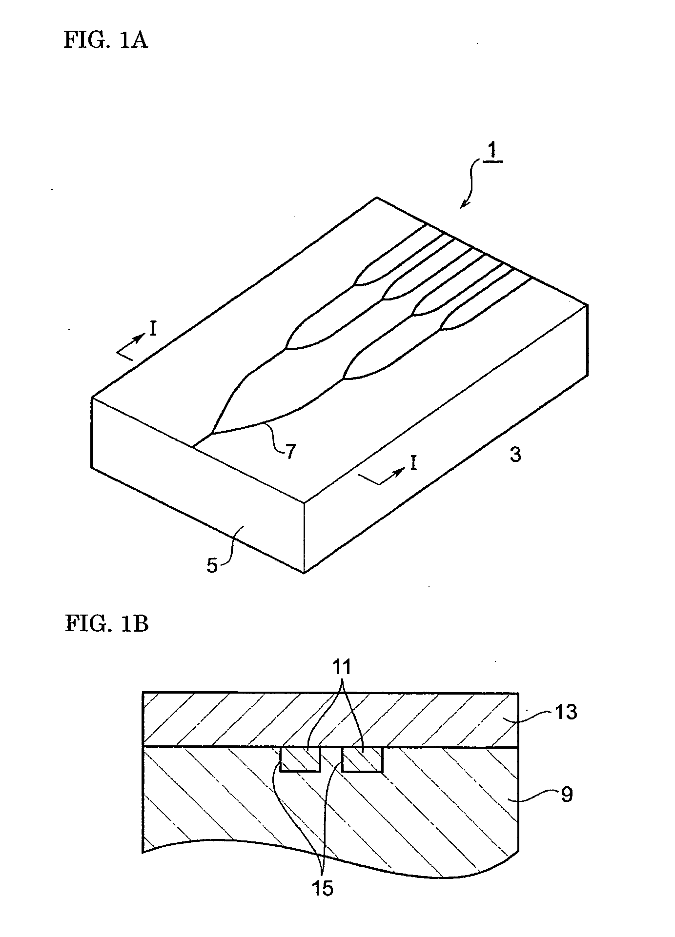
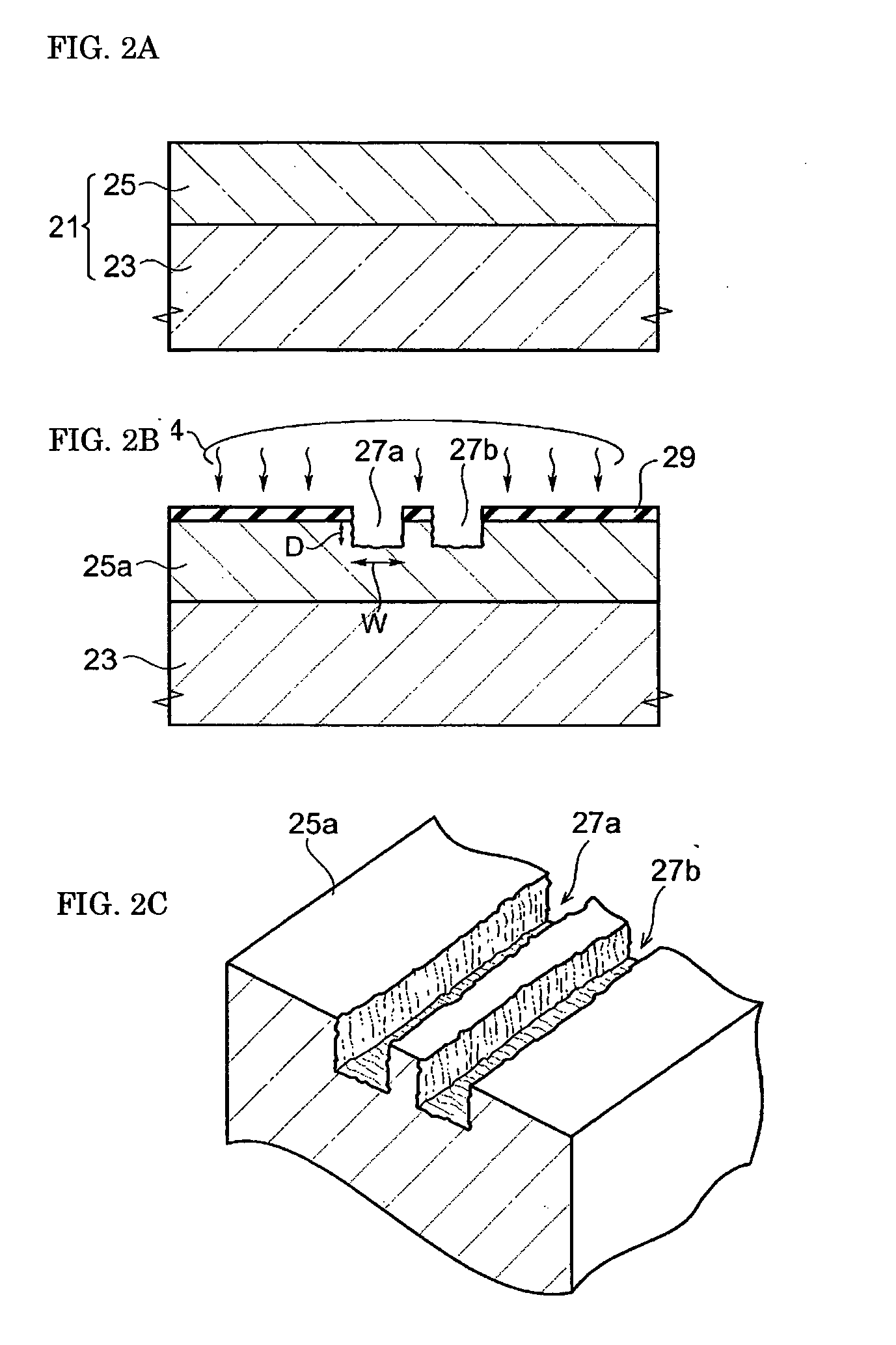
[0014]FIGS. 1A and 1B illustrate a splitter, which is an example of the optical waveguide device manufactured by the method of the present invention. FIG. 1A is a perspective view, and FIG. 1B is a cross sectional view along the I-I line in FIG. 1A. An optical waveguide device 1 includes a supporting substrate 5, and an optical waveguide 7 is provided over the supporting substrate 5. The optical waveguide 7 comprises a glass region serving as an undercladding 9, a core 11, and a glass region serving as an overcladding 13. The top portion of the supporting substrate 5 may serve as the undercladding 9. The glass region serving as the undercladding 9 and the glass region serving as the overcladding 13 include a dopant that is capable of lowering the softening temperature when added. The core 11 is provided inside a groove 15 that is provided on the undercladding 9. The method of the present invention for manufacturing an optical waveguide device reduces bumps and pits on the sides and ...
PUM
 Abstract
Description
Claims
Application Information