ESD-resistant photomask and method of preventing mask ESD damage

Inactive Publication Date: 2005-09-29
TAIWAN SEMICON MFG CO LTD
View PDF3 Cites 4 Cited by
  • Summary
  • Abstract
  • Description
  • Claims
  • Application Information

AI Technical Summary

Benefits of technology

[0017] In accordance with these and other objects and advantages, the present invention is generally directed to an ESD-resistant photomask which is used to transfer a circuit pattern onto a photoresist layer provided on a semiconductor wafer. The photomask includes a mask substrate, a pattern-forming material provided on the substrate, a circuit pattern defined by exposure regions etched in the pattern-forming material, and positive or negative ions implanted into the mask substrate throughout ion implantation regions. The ion implantation regions typically span the exposure regions in the mask. The ions in the ion implantation regions dissipate electrostatic charges on the mask, thus preventing the buildup of electrostatic charges which could otherwise attract image-distorting particles to the mask or damage the mask.

Problems solved by technology

The reticle may be easily damaged such as by dropping of the reticle, the formation of scratches on the reticle surface, electrostatic discharge (ESD), and particles.
ESD can cause discharge of a small current through the chromium lines on the surface of the reticle, melting a circuit line and destroying the circuit pattern.
Consequently, the circuit pattern image transferred through the mask can be distorted, compromising pattern reliability and causing severe yield loss.
One of the problems inherent in the conventional use of multiple ESD eliminators mounted beneath the ceiling of the cleanroom is that many areas in the cleanroom lack sufficient downflow of air to facilitate sufficient transfer of the neutralizing ions from the ESD eliminators to the surfaces of the reticles.
This increases the likelihood of ESD-induced damage to the reticles as they are carried or transported from the reticle stocker to the step-and-scan system and as they await their turn for the step-and-scan procedure.

Method used


Image

  • ESD-resistant photomask and method of preventing mask ESD damage
  • ESD-resistant photomask and method of preventing mask ESD damage
  • ESD-resistant photomask and method of preventing mask ESD damage

Examples


Embodiment Construction

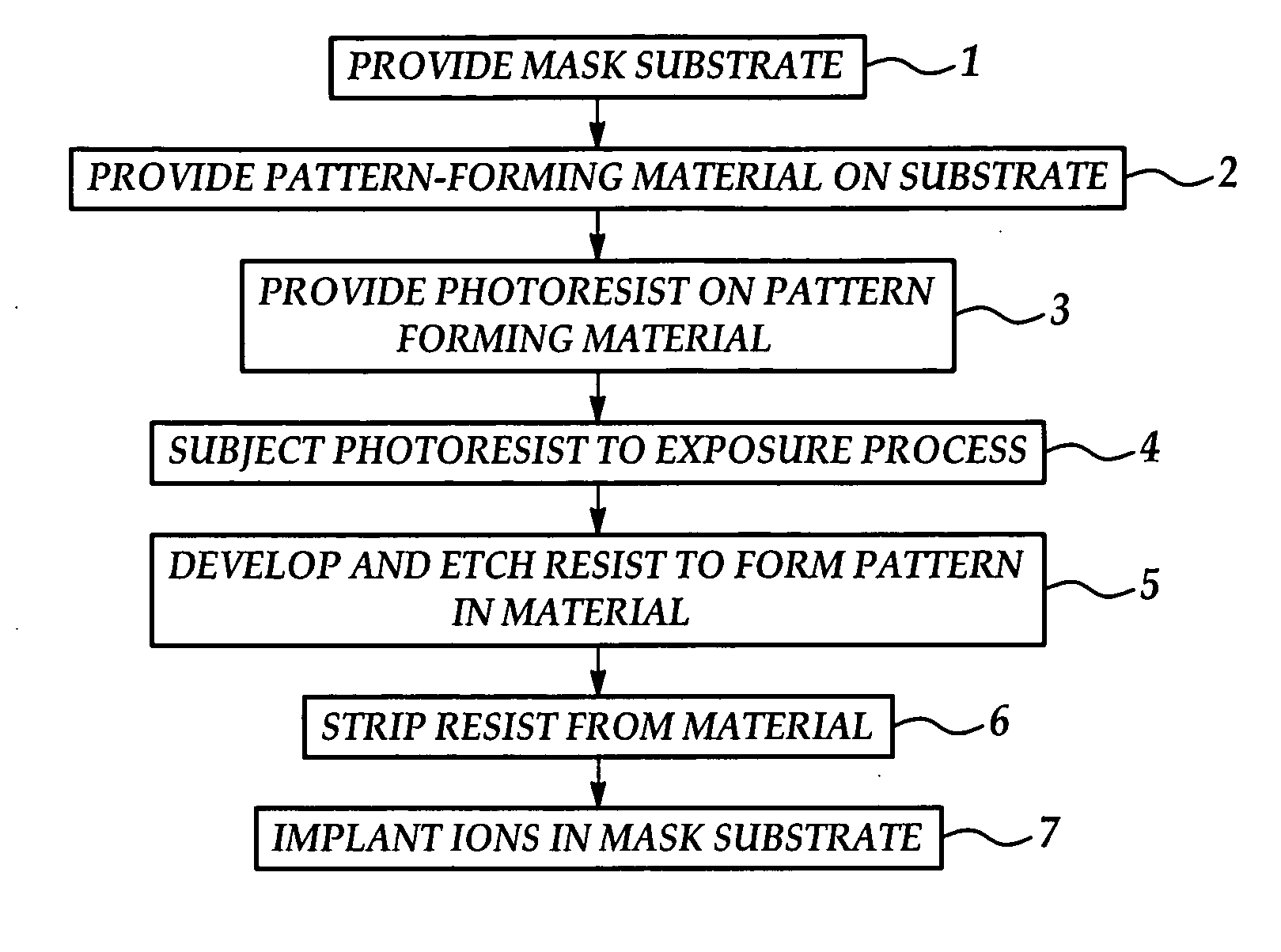
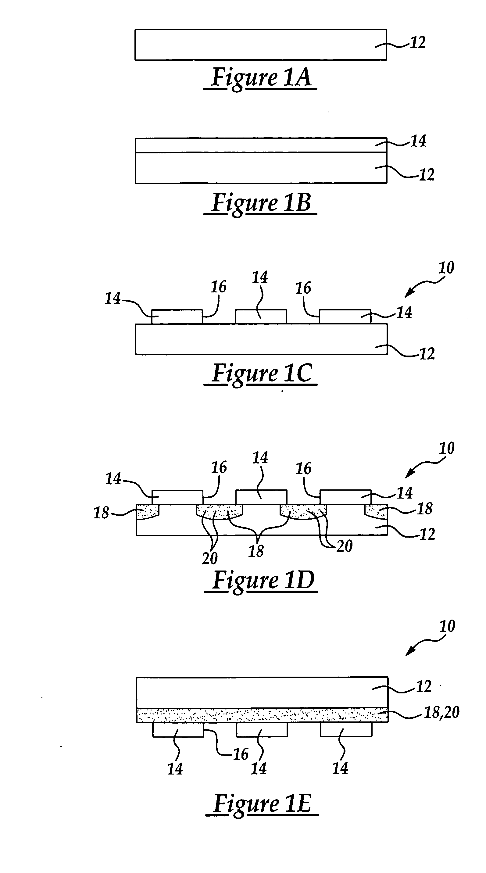
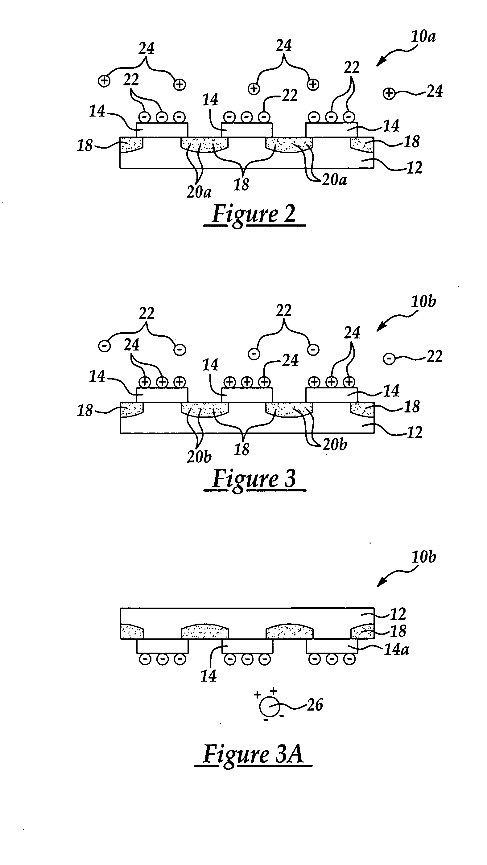
[0030] The present invention contemplates an ESD-resistant photomask for transferring a circuit pattern onto a photoresist layer provided on a semiconductor wafer during the photolithography stage of integrated circuit fabrication. The ESD-resistant photomask includes a transparent mask substrate, a pattern-forming material deposited on the substrate, light-transmissive exposure regions etched in the pattern-forming material to define a circuit pattern, and positive or negative ions implanted into the substrate throughout ion implantation regions which typically span the exposure regions in the mask. Electrostatic charges on the mask are dissipated by the ions in the ion implantation regions, thus preventing the buildup of electrostatic charges which could otherwise attract image-distorting particles to the mask or damage the mask.

[0031] The method of the present invention further includes a novel method for preventing or at least substantially reducing ESD-induced damage to a phot...


PUM


Abstract

An ESD-resistant photomask and method of preventing mask ESD damage is disclosed. The ESD-resistant photomask includes a mask substrate, a pattern-forming material provided on the substrate, a circuit pattern defined by exposure regions etched in the pattern-forming material, and positive or negative ions implanted into the mask substrate throughout ion implantation regions. The ions in the ion implantation regions dissipate electrostatic charges on the mask, thus preventing the buildup of electrostatic charges which could otherwise attract image-distorting particles to the mask or damage the mask.

Description

FIELD OF THE INVENTION [0001] The present invention relates to photomasks used to transfer a circuit pattern onto a semiconductor wafer in the fabrication of integrated circuits. More particularly, the present invention relates to an electrostatic discharge (ESD) resistant photomask and method of preventing electrostatic discharge (ESD) damage to a photomask by implanting ions into the mask substrate to dissipate electrostatic charges on the mask. BACKGROUND OF THE INVENTION [0002] The fabrication of various solid state devices requires the use of planar substrates, or semiconductor wafers, on which integrated circuits are fabricated. The final number, or yield, of functional integrated circuits on a wafer at the end of the IC fabrication process is of utmost importance to semiconductor manufacturers, and increasing the yield of circuits on the wafer is the main goal of semiconductor fabrication. After packaging, the circuits on the wafers are tested, wherein non-functional dies are...

Claims


Application Information

Patent Timeline
IPC IPC(8): G03C5/00G03F1/14G03F9/00G21K5/10H01J37/08
CPCG03F1/14G03F1/144H01J2237/31794G03F1/60G03F1/40
Inventor CHANG, CHING-YU
Owner TAIWAN SEMICON MFG CO LTD
Why Eureka
Try Eureka