Flexible printed circuits with many tiny holes

a printed circuit and small hole technology, applied in printed circuit dielectrics, porous dielectrics, liquid/solution decomposition chemical coatings, etc., can solve the problems of high component density, high cost of manufacturing lithography-based pcb's, and high cost of manufacturing fp

Inactive Publication Date: 2005-10-06
MAHARSHAK ARIE +2
View PDF34 Cites 31 Cited by
  • Summary
  • Abstract
  • Description
  • Claims
  • Application Information

AI Technical Summary

Benefits of technology

[0009] Embodiments of the invention may include a switch having for example a board with for example a plurality of holes running through such board from a first side to a second side. A conductive material may be applied to such board so that such material may for ex...

Problems solved by technology

Generally, the cost of manufacturing lithography based PCB's is substantial.
However, there are applications in which high component density is not desired, but the cost of manufacturing the FPC is critical to the commercial success of the product.
Most often, production of such a consumer electronic product demands intricate manufacturing techniques for inserting components in between the thickness of a sheet, the removal of special cutouts, the addition of spacers and unusual bookbinding methods.
Therefore, the cost of these devices may...

Method used


Image

  • Flexible printed circuits with many tiny holes
  • Flexible printed circuits with many tiny holes
  • Flexible printed circuits with many tiny holes

Examples


Embodiment Construction

[0024] In the following detailed description, numerous specific details are set forth in order to provide a thorough understanding of the invention. However, it will be understood by those skilled in the art that the present invention may be practiced without these specific details. In other instances, well-known methods, procedures, and components have not been described in detail so as not to obscure the present invention.

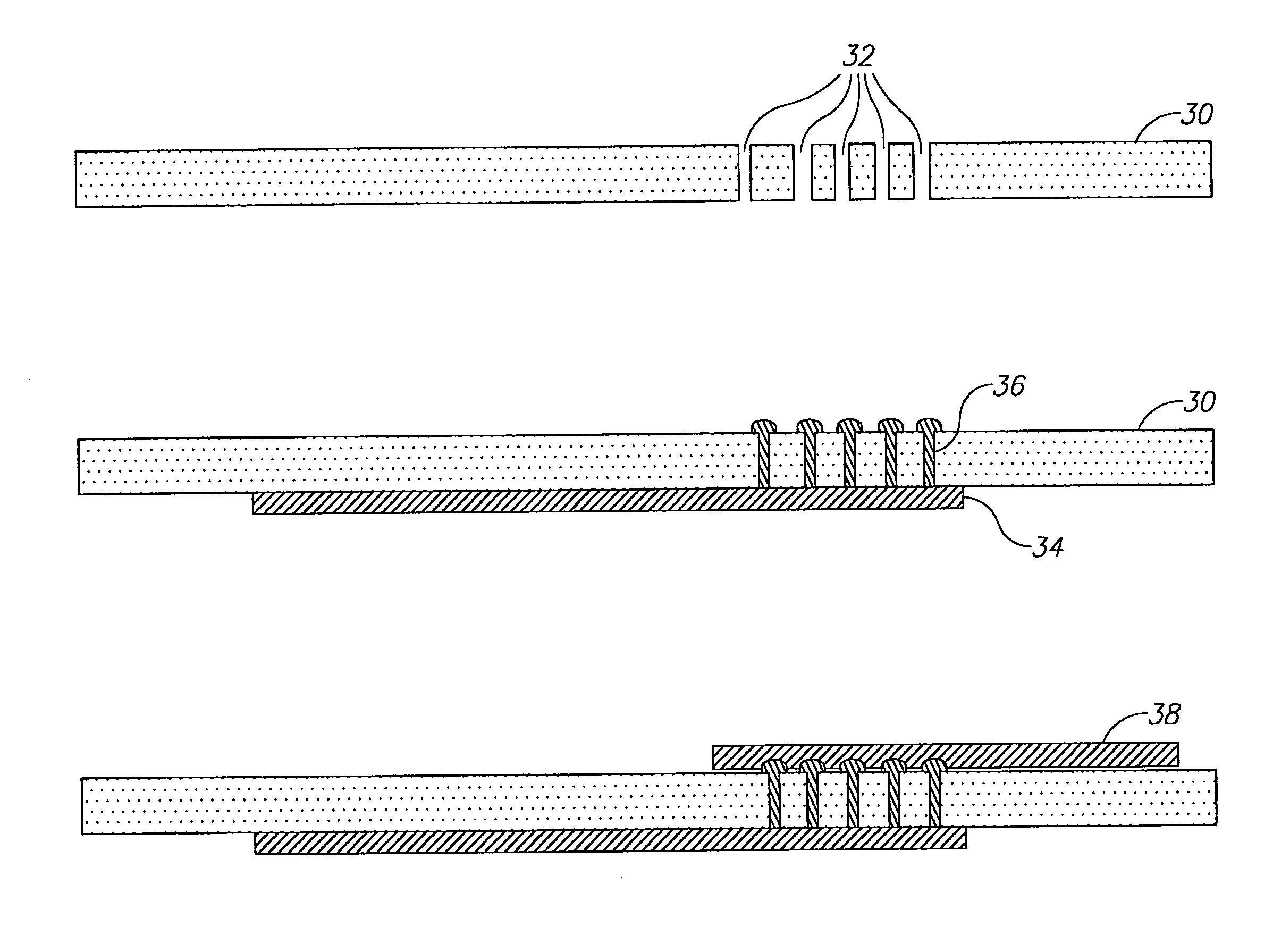
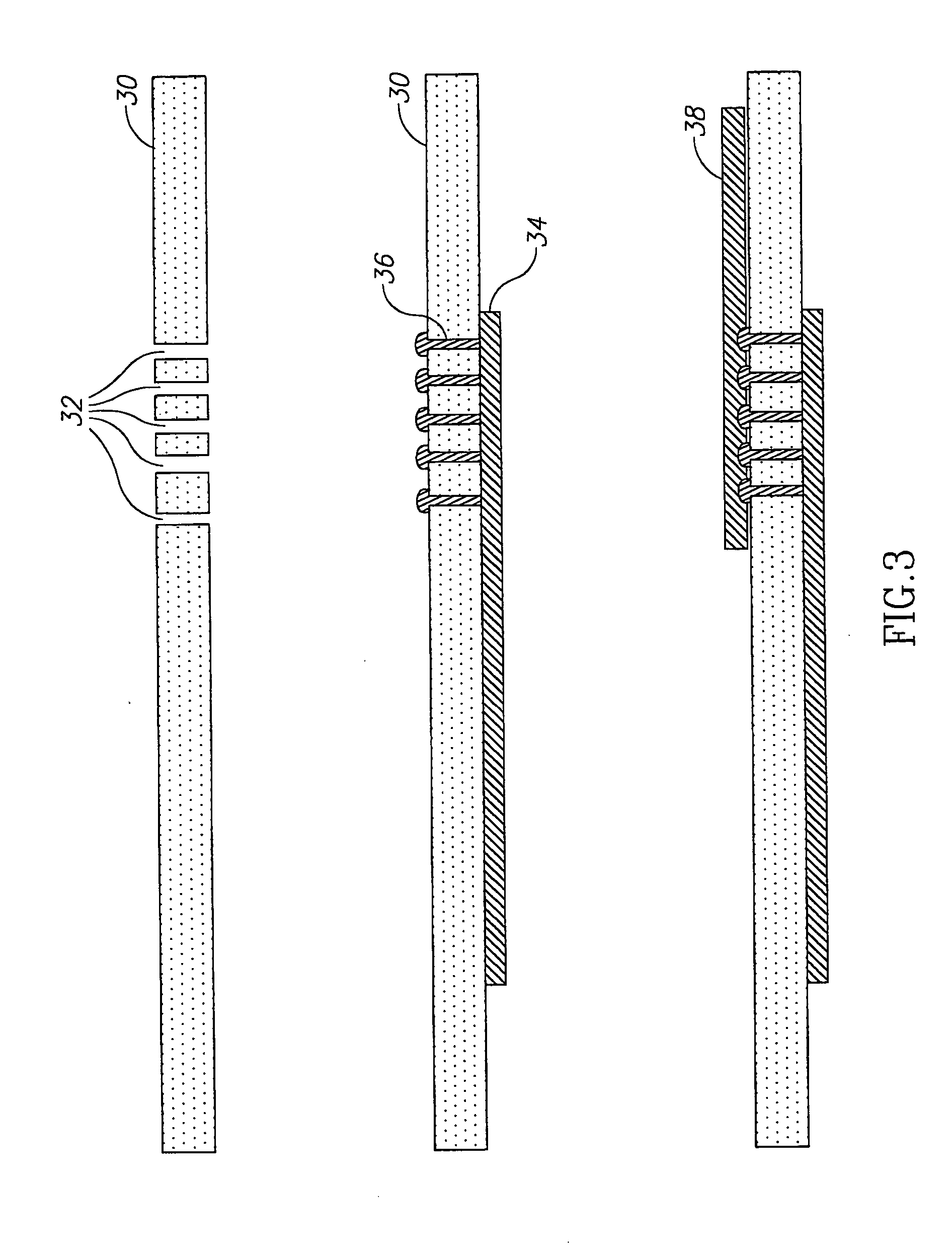
[0025] Reference is made to FIG. 3 a method for producing via connections in FPC in accordance with an embodiment of the invention. In some embodiments, a thin, flexible, non-conductive substrate 30 such as for example paper, plastic, or other suitable material, may be fashioned with a set or array of tiny holes 32 in the location where a first conductive area such as for example a conductive line 34 and second conductive line 38 are to overlap on opposing sides of substrate 30 and make an electrical connection, or in the location where the substrate 30 is subje...


PUM

PropertyMeasurementUnit
Diameteraaaaaaaaaa
Thicknessaaaaaaaaaa
Forceaaaaaaaaaa

Abstract

A board that may include for example a first conductive area on a first side and a second conductive area on a second side of such board. The board may be fitted with a plurality of holes that may for example open or end on both such first side and such second side of such board. A conductive material in the form of for example a liquid or gel may be applied or for example painted onto one or both sides of such board so that such material may for example substantially fill some or all of such holes and may establish a connection through which an electric current may pass from for example the first conductive area to the second conductive area. A switch having for example a board with a plurality of holes running through such board from a first side to a second side. A conductive material may for example be applied to such board so that such material substantially fills for example two or more of such holes and may be capable of forming an electrical connection between a conductive area on a first side of such board and a conductive area on a second side of such board. A method of forcing a conductive liquid into a plurality of holes in a board so that the liquid forms for example a connection capable of carrying a current between a conductive area on a first side of such board and a conductive area of a second side of such board.

Description

FIELD OF THE INVENTION [0001] The present invention relates in general to methods of producing flexible printed circuits, and particularly to producing flexible printed circuits with many tiny holes. BACKGROUND OF THE INVENTION [0002] Electronic printed circuits board (PCB) and flexible printed circuits (FPC) are known. High component density is available through the use of fine line lithography and multi-layer PCB. Generally, the cost of manufacturing lithography based PCB's is substantial. However, there are applications in which high component density is not desired, but the cost of manufacturing the FPC is critical to the commercial success of the product. In some applications, the size of the FPC is determined by the shape of the product and not by the area needed to position the few electronic components. Examples for such products are toys, electronic books and other consumer products. Cheap flexible circuits may be used, among other uses, in alarm systems for card holders as...

Claims


Application Information

Patent Timeline
IPC IPC(8): C23C18/00H01R12/04H01R24/00H01R33/00H05K1/00H05K1/11H05K3/40
CPCH05K1/0287H05K1/0393H05K3/4069H05K2201/0116Y10T29/49124H05K2203/0139H05K2203/0278H05K2203/1572H05K2201/09609
Inventor MAHARSHAK, ARIEMAHARSHAK, TOMERMAHARSHAK, NITSAN
Owner MAHARSHAK ARIE
Why Eureka
Try Eureka