Back end IC wiring with improved electro-migration resistance

a back-end ic and wiring technology, applied in the direction of semiconductor devices, semiconductor/solid-state device details, electrical apparatus, etc., can solve the problems of increasing processing complexity, increasing the cost and complexity of processing, and tungsten electrical performance properties, including electrical resistance, are not enough for characteristic device dimensions, etc., to improve electrical properties and reliability of wiring interconnects

Inactive Publication Date: 2005-10-06
TAIWAN SEMICON MFG CO LTD
View PDF4 Cites 20 Cited by
  • Summary
  • Abstract
  • Description
  • Claims
  • Application Information

AI Technical Summary

Benefits of technology

[0006] To achieve the foregoing and other objects, and in accordance with the purposes of the present invention, as embodied and broadly described herein, the present invention provides a multi-level semiconductor device wiring interconnect structure and method of forming the same to improve electrical properties and reliability of wiring interconnects including an electromigration resistance and electrical resistance.

Problems solved by technology

As device characteristic dimensions shrink, however, the prior art practice of forming tungsten plugs in lower metallization layers creates several problems.
For example, the cost and complexity of processing increases, requiring increasing complex processing including tungsten deposition, tungsten dry etchback and / or CMP planarization processes to avoid respectively, for example, voids in tungsten plugs, tungsten particle contamination, and the formation of tungsten metal stringers.
In addition, the electrical performance properties of tungsten, including electrical resistance are less than adequate for characteristic device dimensions less than about 0.25 microns.
Moreover, the high temperature deposition processes currently required for tungsten as well as overlying conventional copper metallization leads to undesirable defects in previously deposited metallization layers.

Method used


Image

  • Back end IC wiring with improved electro-migration resistance
  • Back end IC wiring with improved electro-migration resistance
  • Back end IC wiring with improved electro-migration resistance

Examples


Embodiment Construction

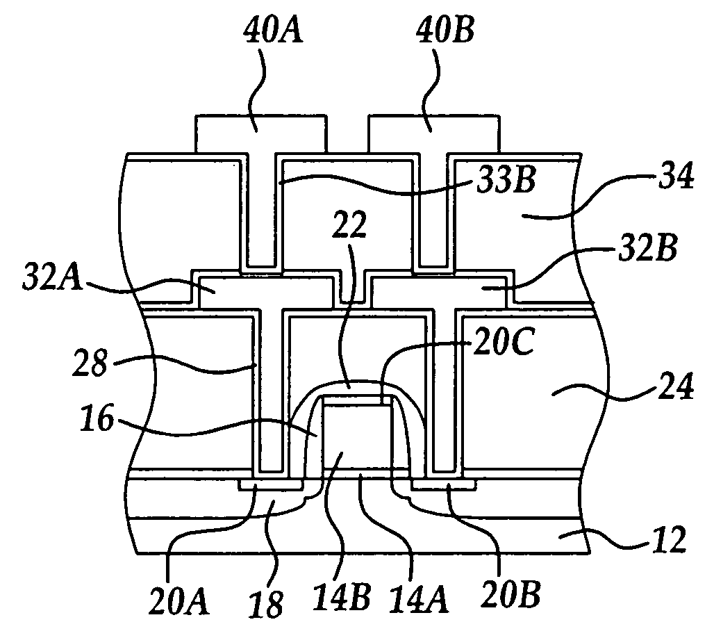
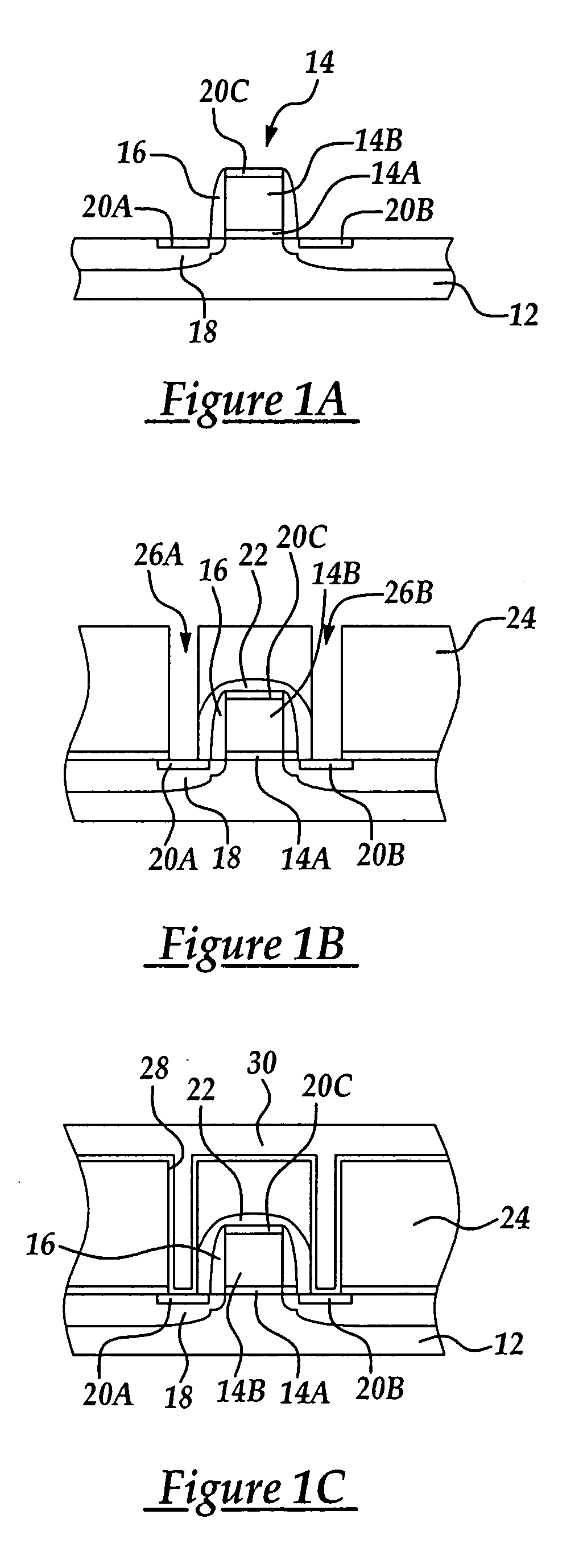
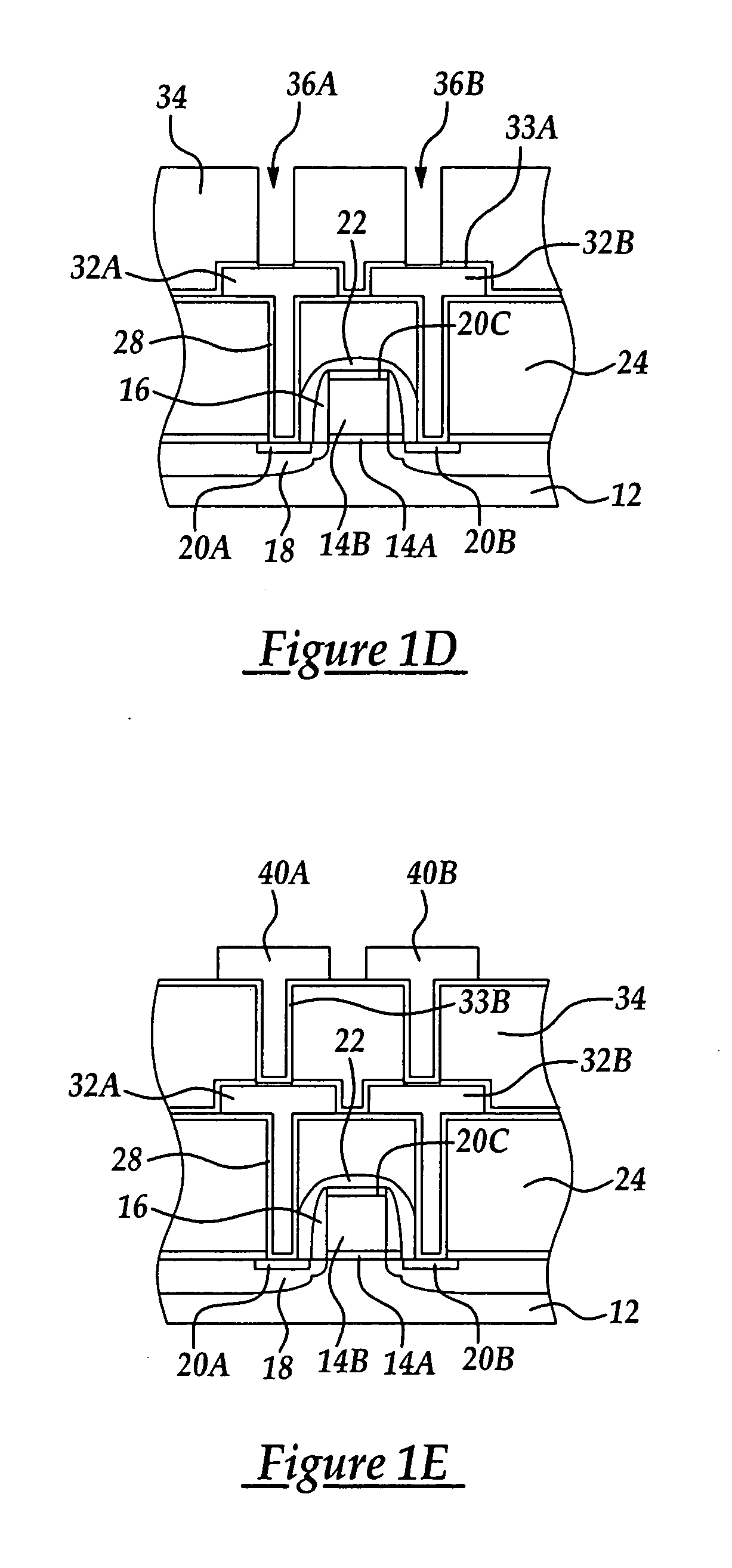
[0012] Although the method of the present invention is explained by reference to an exemplary generic multi-level integrated it including CMOS transistor devices, it will be appreciated that the method of the present invention is particularly applicable to formation of logic circuits, and y circuits, including heterogeneous integrated circuits as mixed signal circuitry including analog conditioning circuitry and combinations of the foregoing, where the advantages of increased electromigration resistance, reduced RC delay time constant, and reduced via contact resistance are particularly advantageous. In addition, although the method of the present invention may be applied to integrated circuits with characteristic dimensions greater than about 0.25 microns, the structure and method of the present invention is particularly advantageous for integrated circuits with characteristic device dimensions less than about 0.25 microns, including 0.18 microns and 0.13 microns.

[0013] Referring ...


PUM


Abstract

A multi-level semiconductor device wiring interconnect structure and method of forming the same to improve electrical properties and reliability of wiring interconnects including an electromigration resistance and electrical resistance, the method including forming a dielectric insulating layer over a conductive portion; forming a via opening in closed communication with the conductive portion; forming a first barrier layer to line the via opening; forming a layer of AlCu according to a sputtering process to fill the via opening to form an AlCu via including a portion overlying the first dielectric insulating layer; and, photolithographically patterning and dry etching the portion to form an AlCu interconnect line over the AlCu via.

Description

FIELD OF THE INVENTION [0001] This invention generally relates to large scale integrated circuit (LSI) processing methods including formation of metallization interconnects and more particularly to an improved method and structure for wiring a multi-level semiconductor device. BACKGROUND OF THE INVENTION [0002] Metallization interconnects are critical to the proper electronic function of semiconductor devices. Several advances in integrated circuit manufacturing processing have been aimed at improving signal transport speed by reducing metal interconnect resistivities and improving resistance to electromigration effects. Copper has increasingly become a metal of choice in, for example, upper levels of metallization in a multi-level semiconductor device due to its low resistivity. Tungsten (W), however, has been used in the lower metallization layers, for example the PMD layer to form plugs or vias to contact underlying conductive areas including CMOS source and drain regions since i...

Claims


Application Information

Patent Timeline
Patent Type & Authority Applications(United States)
IPC IPC(8): H01L21/3205H01L21/8238H01L23/532H01L21/44H01L21/4763H01L21/768
CPCH01L21/76838H01L21/76877H01L23/53223H01L2924/0002H01L2924/00
Inventor HUANG, CHIEN-CHAO
Owner TAIWAN SEMICON MFG CO LTD
Why Eureka
Try Eureka