Crystalline oxide semiconductor thin film, and method of forming the same and thin film transistor and method of manufacturing the same and display panel and electronic device

a technology of crystalline oxide semiconductor and thin film, which is applied in the direction of semiconductor devices, electrical devices, basic electric elements, etc., can solve the problems of limiting the improvement of electrical properties and stability, and achieve the effect of improving electrical properties and reliability

Active Publication Date: 2022-06-30
ADRC CO KR
View PDF12 Cites 0 Cited by
  • Summary
  • Abstract
  • Description
  • Claims
  • Application Information

AI Technical Summary

Benefits of technology

[0026]A crystalline oxide semiconductor thin film and a thin film transisto

Problems solved by technology

However, oxide semiconductors are mostly included in an amorphous state, and in th

Method used


Image

  • Crystalline oxide semiconductor thin film, and method of forming the same and thin film transistor and method of manufacturing the same and display panel and electronic device
  • Crystalline oxide semiconductor thin film, and method of forming the same and thin film transistor and method of manufacturing the same and display panel and electronic device
  • Crystalline oxide semiconductor thin film, and method of forming the same and thin film transistor and method of manufacturing the same and display panel and electronic device

Examples


example 1

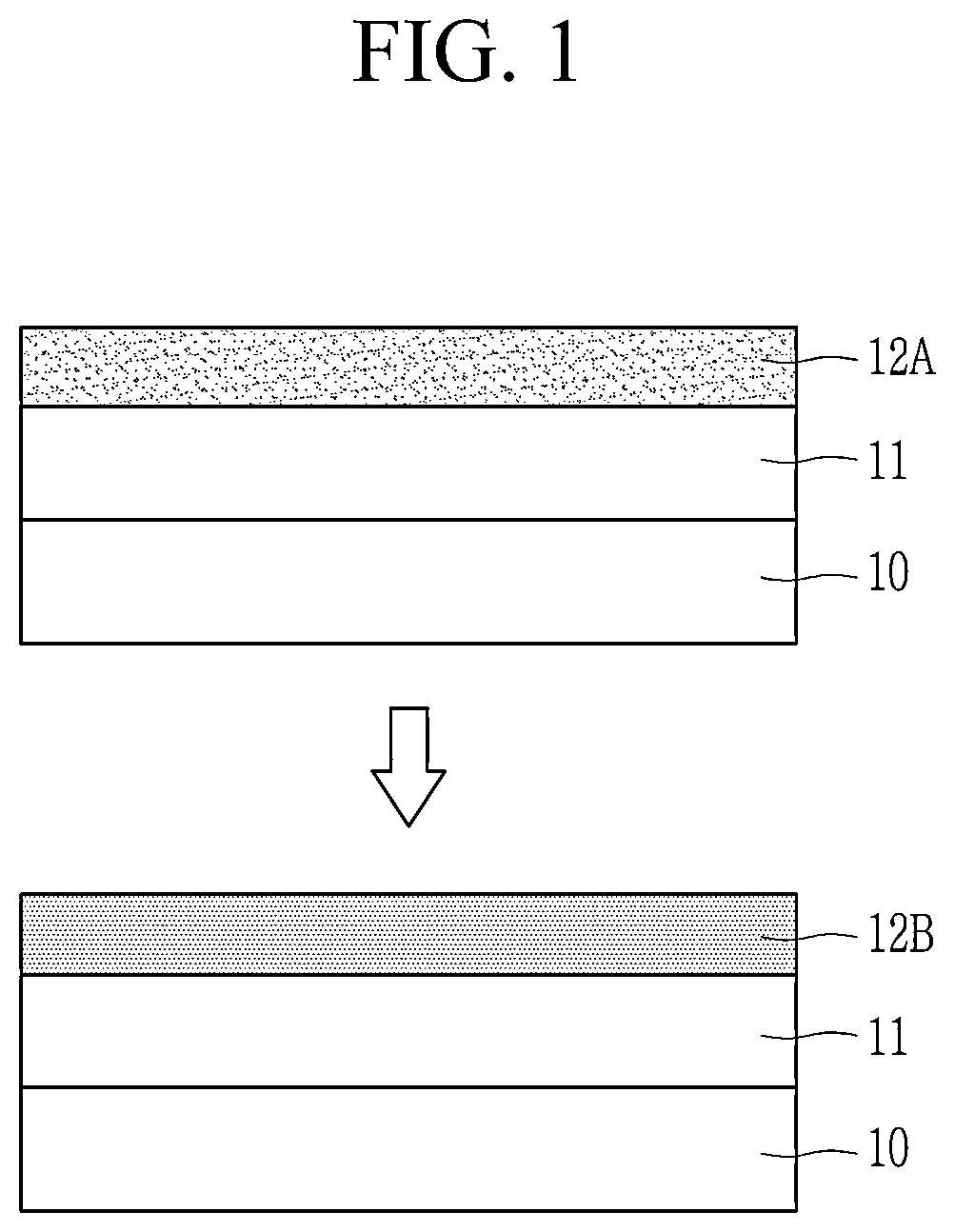
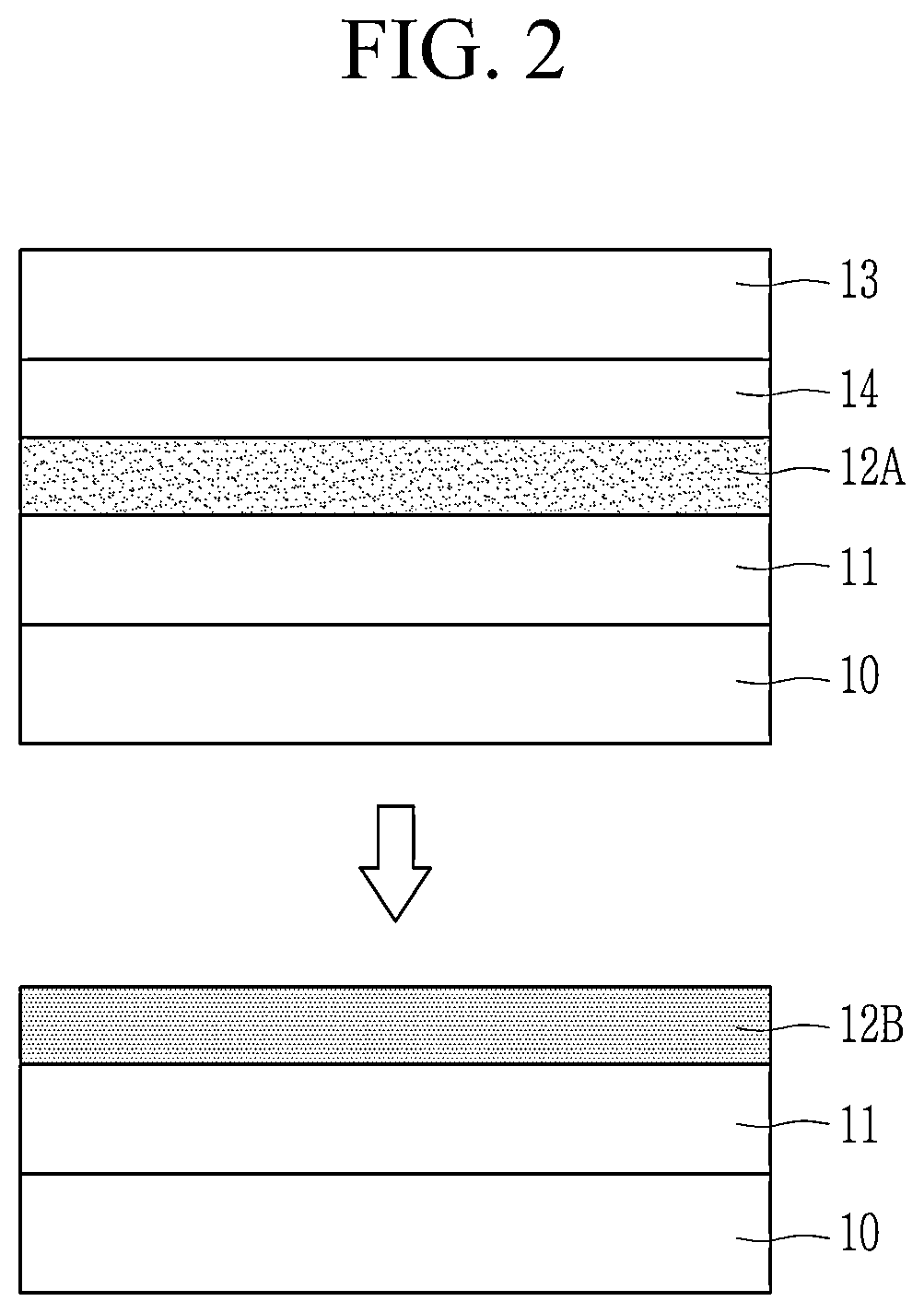
[0114]A 500 nm-thick buffer layer is formed on a glass substrate by depositing a silicon oxide through chemical vapor deposition (CVD). Subsequently, on the buffer layer, an indium-gallium-tin oxide is formed through RF sputtering to form a 50 nm-thick amorphous indium-gallium-tin oxide (IGTO) thin film. Subsequently, the IGTO thin film is put in a furnace and annealed at 700° C. (rising time: 2 hours) for 30 minutes to form a crystalline oxide semiconductor thin film.

example 2

[0115]A crystalline oxide semiconductor thin film is formed according to the same method as Example 1 except that a 100 nm-thick amorphous IGTO thin film is formed instead of the 50 nm-thick amorphous IGTO thin film, and the annealing time is changed to 2 hours.

Evaluation I

[0116]Crystallinity of the crystalline oxide semiconductor thin films according to Examples 1 and 2 are evaluated.

[0117]FIG. 5 is a transmission electron microscopic (TEM) photograph of the crystalline oxide semiconductor thin film according to Example 1, and FIG. 6 is an XRD graph of the crystalline oxide semiconductor thin film according to Examples 1 and 2.

[0118]Referring to FIGS. 5 and 6, the crystalline oxide semiconductor thin films according to Examples 1 and 2 have crystals with a c-axis oriented crystal plane and exhibit a 009 diffraction peak (2θ≈around about 31°).

Formation of Crystalline Oxide Semiconductor Thin Film II

example 3

[0119]On a glass substrate, a silicon oxide is deposited through the chemical vapor deposition (CVD) to form a 200 nm-thick buffer layer. Subsequently, on the buffer layer, an indium-gallium-tin oxide is deposited through RF sputtering to form a 50 nm-thick amorphous indium-gallium-tin oxide (IGTO) thin film. The IGTOthin film is annealed by using RTA equipment for 10 minutes or 30 minutes at 800° C. (rising time: 2 minutes) to form a crystalline oxide semiconductor thin film.


PUM


Abstract

Disclosed are a crystalline oxide semiconductor thin film including a crystalline oxide semiconductor including indium, gallium, and tin, the crystalline oxide semiconductor exhibiting a (009) diffraction peak in an X-ray diffraction spectrum, and a method of forming the same, a thin film transistor and a method of manufacturing the same, a display panel, and an electronic device.

Description

CROSS-REFERENCE TO RELATED APPLICATION[0001]This application claims priority to and the benefit of Korean Patent Application No. 10-2020-0186260 filed in the Korean Intellectual Property Office on Dec. 29, 2020, the entire contents of which are incorporated herein by reference.BACKGROUND1. Field[0002]A crystalline oxide semiconductor thin film and a method of forming the same, a thin film transistor and a method of manufacturing the same, and a display panel and an electronic device are disclosed.2. Description of the Related Art[0003]A display device such as a liquid crystal display (LCD) or an organic light emitting diode display (OLED display) includes a thin film transistor (TFT) that is a three-terminal device as a switching device and / or a driving device. Recently, as such a thin film transistor, a thin film transistor including an oxide semiconductor has been studied. However, oxide semiconductors are mostly included in an amorphous state, and in this case, there is a limit t...

Claims


Application Information

Patent Timeline
IPC IPC(8): H01L27/12
CPCH01L27/1285H01L27/1225H01L29/7869H01L29/66969H01L21/02565H01L21/02609H01L21/0259H01L21/0262H01L21/02628H01L21/02667
Inventor CHOI, SOON HOHWANG, CHAE YEONLEE, SUHUI
Owner ADRC CO KR
Why Eureka
Try Eureka