

Semiconductor storage
a technology of semiconductor storage and storage devices, which is applied in the direction of digital storage, transistors, instruments, etc., can solve the problems of reducing the storage capacity of the device, so as to achieve effective interference restraint in rewrite operation, sufficient memory function, and shorten the distance between these two charge holding portions
- Summary
- Abstract
- Description
- Claims
- Application Information
AI Technical Summary
Benefits of technology
Problems solved by technology
Method used
Image

Examples
first embodiment
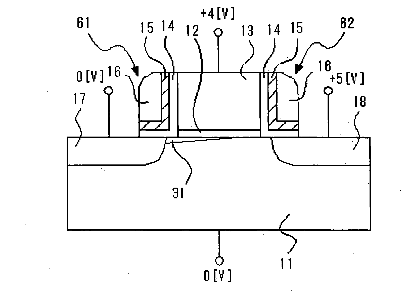
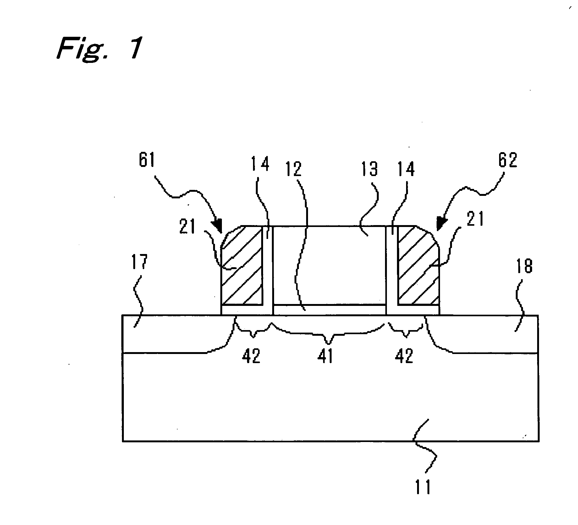
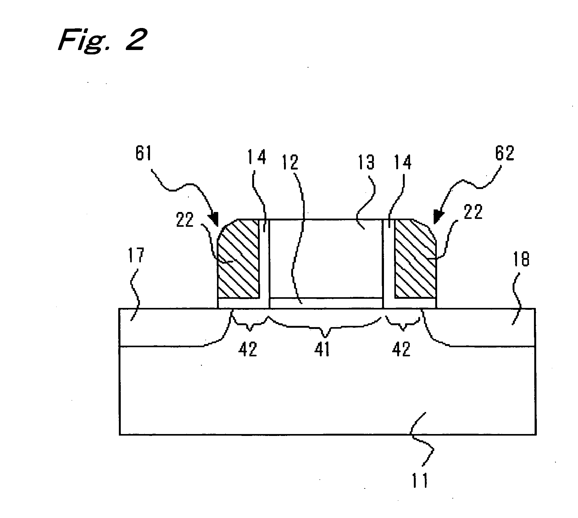
[0105] The structure of a memory device constituting a semiconductor storage device of the present embodiment will be described with reference to FIGS. 1 to 3. FIGS. 1 to 3 are outlined cross sectional views showing memory devices whose structure of a charge holding portion in the shape of side wall spacer is different from each other.
[0106] The memory device constituting the semiconductor storage device of the present embodiment is formed as a nonvolatile memory cell capable of storing two bits, in which, as shown in FIGS. 1 to 3, a gate electrode 13 having a gate length similar to normal transistors is formed on a semiconductor substrate 11 through a gate insulating film 12, and charge holding portions 61, 62 in the shape of side wall spacer are formed on the side walls of the gate insulating film 12 and the gate electrode 13. On the side of the charge holding portions 61, 62 facing the gate electrode 13, there are formed a first diffusion layer region 17 and a second diffusion l...
second embodiment
[0138] In a semiconductor storage device in this embodiment as shown in FIG. 9, charge holding portions 161, 162 are composed of a region for holding electric charges (the region for storing electric charges, which may be a film having a function of holding electric charges) and a region for obstructing release of electric charges (which may be a film having a function of obstructing release of electric charges). The semiconductor storage device has, for example, ONO structure. More specifically, the charge holding portions 161, 162 are structured in the state that a film 142 as a first insulator made of silicon nitride being interposed in between a film 141 as a second insulator made of a silicon oxide and a film 143 as a third insulator made of silicon oxide. Here, the silicon nitride film142 implements a function of storing and holding electric charges. The silicon oxide films 141, 143 implement a function of obstructing release of the electric charges stored in the silicon nitri...
third embodiment
[0153] In this embodiment, a charge holding film 142 as a film made of a first insulator in the charge holding portion 162 has an approximately uniform film thickness as shown in FIG. 14. Further, the charge holding film 142 includes a first portion 181 as a portion having the surface approximately parallel to the surface of the gate insulating film 114 and a second portion 182 as a portion extending in direction approximately parallel to the side face of the gate electrode 117.
[0154] When a positive voltage is applied to the gate electrode 117, electric line of force in the charge holding portion 162 passes the silicon nitride film 142 total two times through the first portion 181 and the second portion 182 as shown with an arrow 183. It is noted that when a negative voltage is applied to the gate electrode 117, the direction of electric line of force is reversed. Herein, a dielectric constant of the silicon nitride film 142 is approx. 6, while a dielectric constant of silicon oxi...
PUM
 Abstract
Description
Claims
Application Information