Method of fabricating high-k dielectric layer having reduced impurity

a dielectric layer and impurity technology, applied in the direction of mechanical equipment, coatings, semiconductor/solid-state device details, etc., can solve the problems of increasing leakage current, deteriorating carrier mobility, increasing leakage current or increasing leakage curren

Active Publication Date: 2005-10-20
SAMSUNG ELECTRONICS CO LTD
View PDF7 Cites 104 Cited by
  • Summary
  • Abstract
  • Description
  • Claims
  • Application Information

AI Technical Summary

Benefits of technology

[0010] Embodiments of the present invention generally provide methods of fabricating a high-k dielectric layer for

Problems solved by technology

In cases where the thickness of the dielectric layer is reduced, however, there often occurs a problem in that leakage current is increased due to the reduced thickness of the dielectric layer.
From this point of view, when one of the foregoing high-k dielectric materials is used as the gate dielectric layer, one or more of the following problems may occur.
In the case of the BST layer, the titanium oxide layer, the tantalum oxide layer, etc., reactivity with a silicon substrate is relatively high; and, thus, the interfacial properties between the gate dielectric layer and the silicon substrate become poor, thereby increasing the leakage current or deteriorating carrier mobility.
In the case of the aluminum oxide layer, thermal stability is relatively high but the dielectric constant is relatively low, so that the resulting improvement in capacitance i

Method used


Image

  • Method of fabricating high-k dielectric layer having reduced impurity
  • Method of fabricating high-k dielectric layer having reduced impurity
  • Method of fabricating high-k dielectric layer having reduced impurity

Examples


experimental examples

[0038]FIGS. 6A and 6B are secondary ion mass spectrometry (SIMS) graphs illustrating a change of impurity content in a dielectric layer over time during the course of a post-treatment step in accordance with this invention. FIG. 6A shows a change of chlorine content, and FIG. 6B shows a change of carbon content. In FIGS. 6A and 6B, the graphs are based on results of the post-treatment for samples under conditions of the following Table 1.

TABLE 1sampleDielectric layerPost-treatmentFirst sample (10)ALD SiO2xSecond sample (11)450° C., heat treatment in O3atomosphereThird sample (12)700° C., heat treatment in N2atomosphereFourth sample (13)750° C., heat treatment in O2atomosphereFifth sample (14)750° C., heat treatment in NH3atomosphereSixth sample (15)750° C., heat treatment in NH3atmosphere + heat treatment inO2 atomosphereSeventh sample (20)700° C., heat treatment in N2atomosphereEighth sample (21)500° C., heat treatment in O2atomosphereNinth sample (22)600° C., heat treatment in O...


PUM

PropertyMeasurementUnit
Thicknessaaaaaaaaaa
Dielectric polarization enthalpyaaaaaaaaaa

Abstract

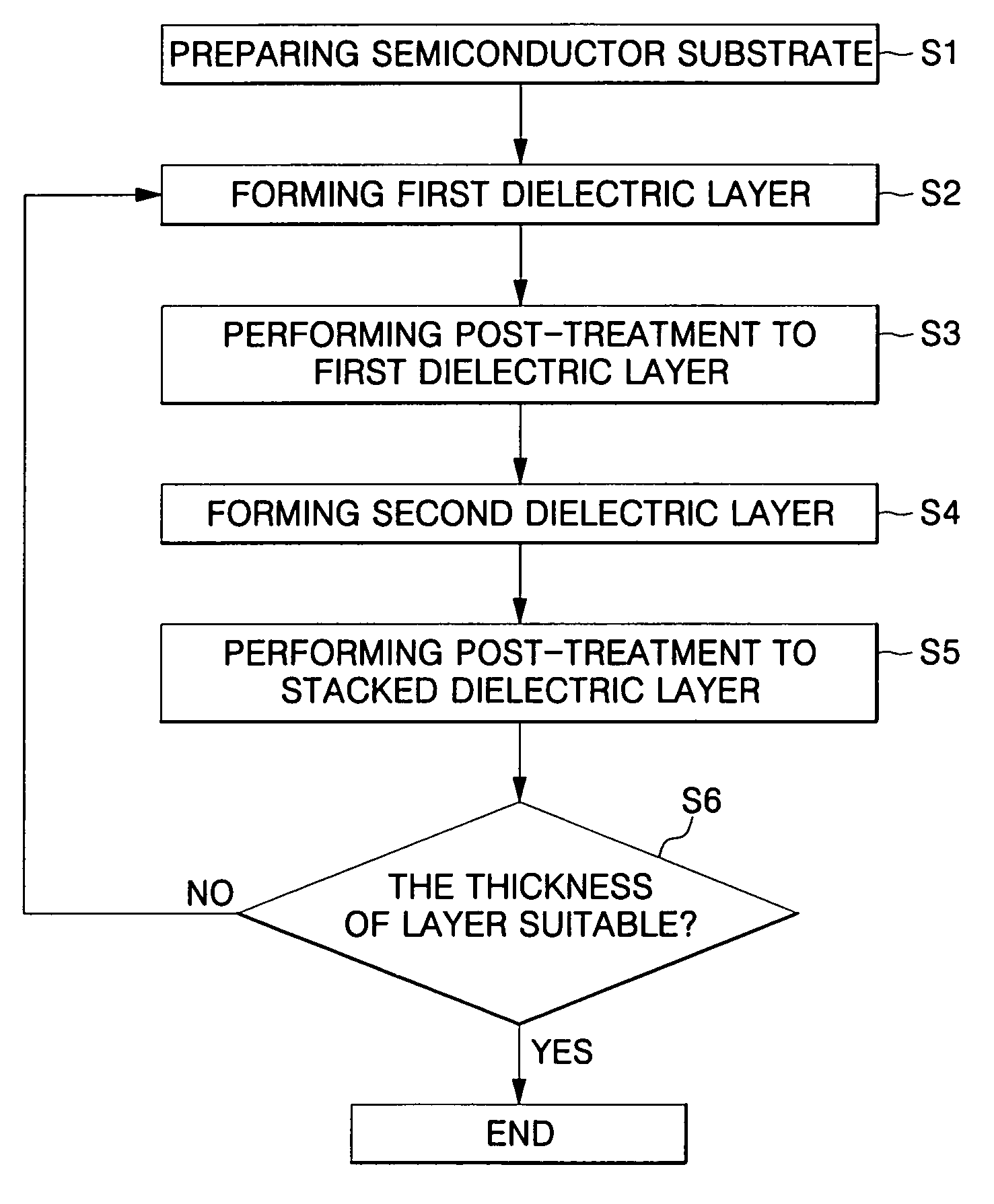
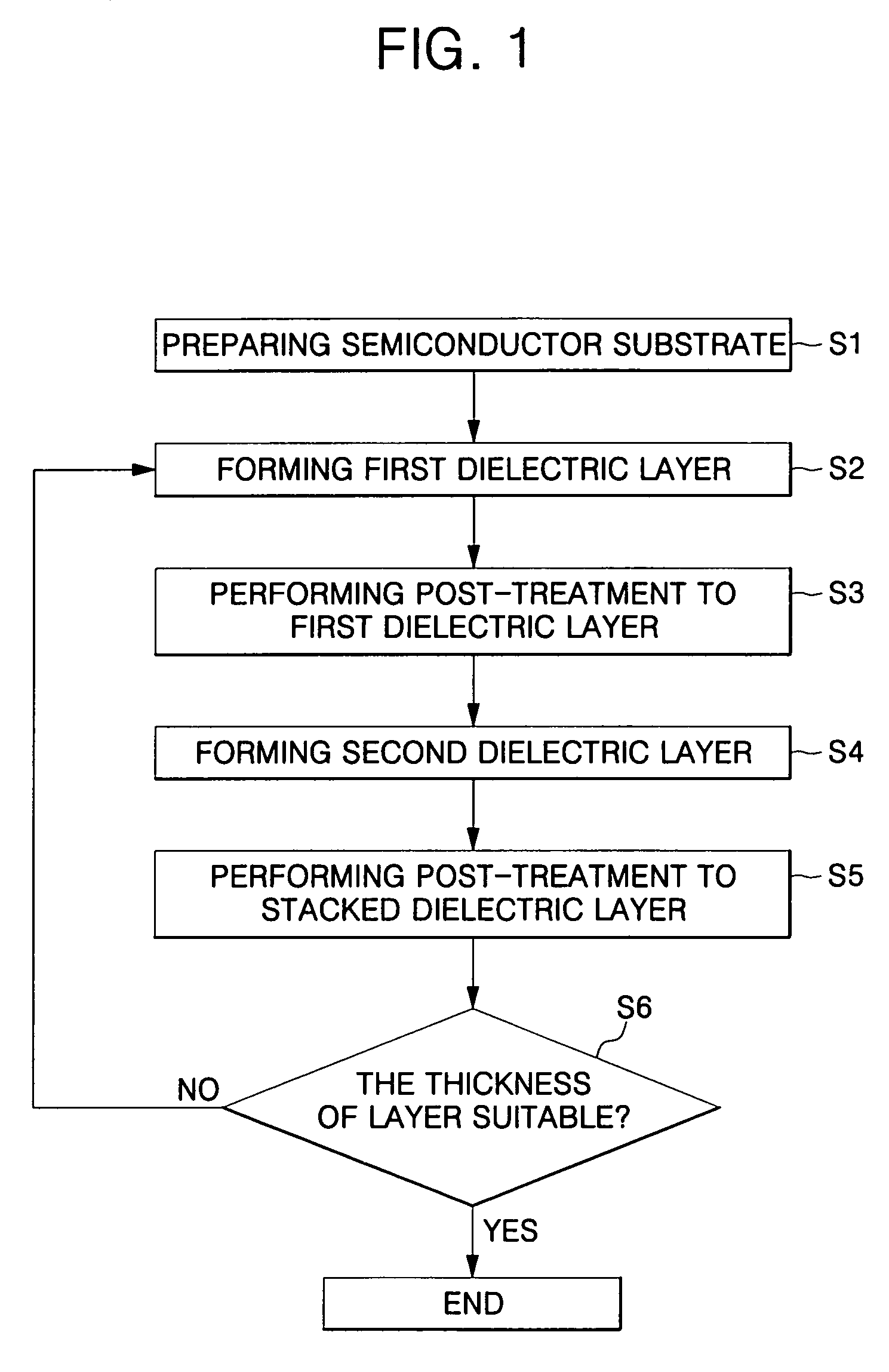
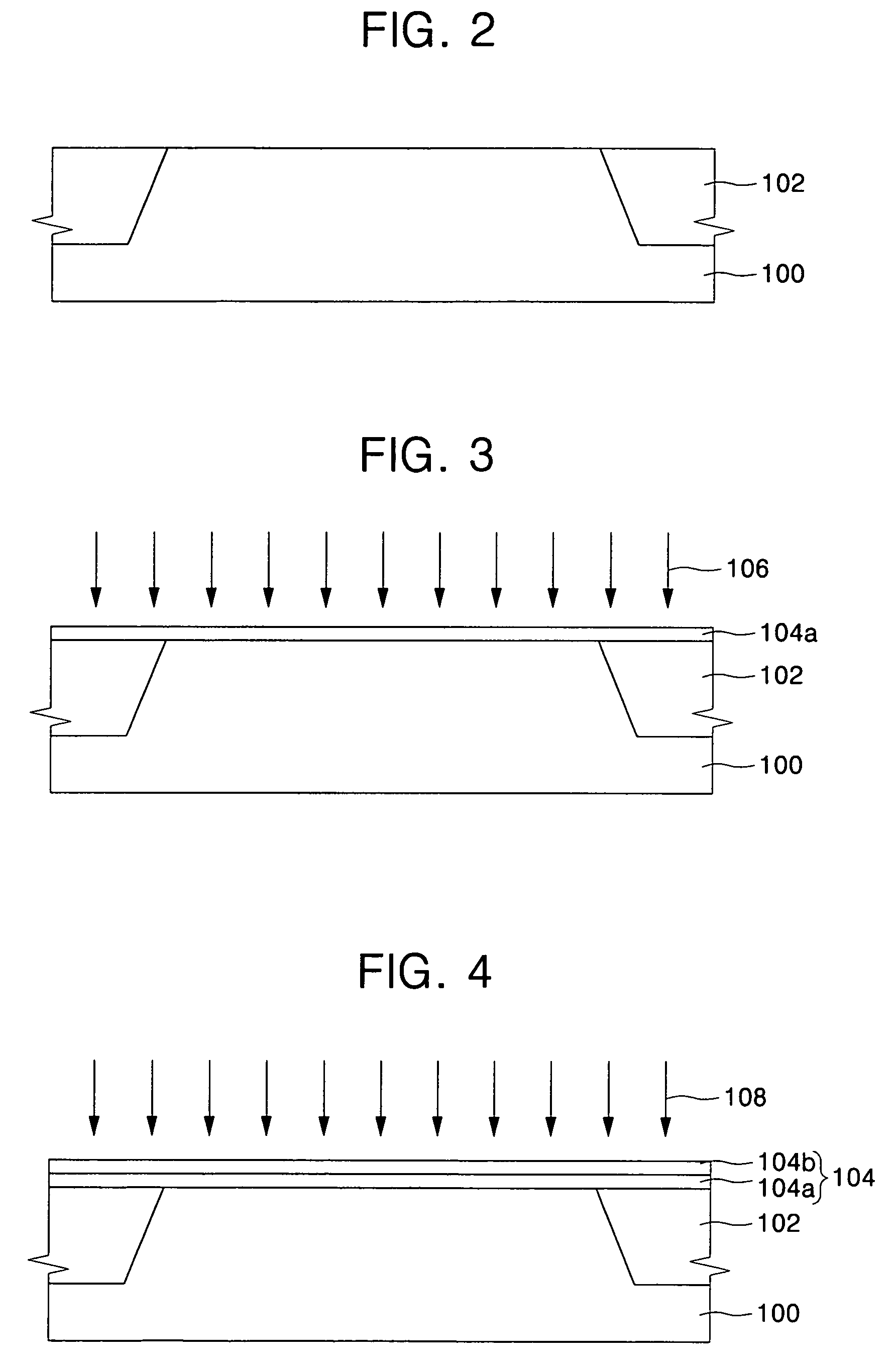
Methods of fabricating high-k dielectric layers having reduced impurities for use in semiconductor applications are disclosed. The methods include the steps of: forming a stacked dielectric layer having a first dielectric layer and a second dielectric layer formed on a semiconductor substrate using an ALD method, in combination with a post-treatment step performed to the stacked dielectric layer. The steps of forming the stacked dielectric layer and performing the post-treatment are repeated at least once, thereby fabricating the high-k dielectric layer.

Description

CROSS-REFERENCE TO RELATED APPLICATION [0001] This application claims the benefit of Korean Patent Application No. 2004-26690, filed Apr. 19, 2004, the contents of which are hereby incorporated herein by reference in their entirety. BACKGROUND OF THE INVENTION [0002] 1. Field of the Invention [0003] The present invention relates to methods of fabricating a dielectric layer used in a semiconductor device and, more particularly, to methods of fabricating a high-k dielectric layer having reduced impurities. [0004] 2. Description of the Related Art [0005] In a semiconductor device, a dielectric layer has a variety of uses. Typically, the dielectric layer is used as a gate dielectric layer of a MOS field effect transistor. To normally operate the semiconductor device, the gate dielectric layer should be able to maintain the capacitance (C) of the device at a suitable level. The capacitance of the dielectric layer is defined as follows: C=ε·A / d (where C is capacitance, ε is a dielectric c...

Claims


Application Information

Patent Timeline
IPC IPC(8): C23C16/40H01L21/28H01L21/314H01L21/31H01L21/336H01L21/469H01L29/51
CPCC23C16/402C23C16/45525C23C16/45527C23C16/45529H01L21/28185H01L29/518H01L21/3142H01L21/3143H01L29/513H01L29/517H01L21/28194H01L21/02318H01L21/022H01L21/0228F15B21/14F15B2211/20515F15B2211/25F15B2211/255
Inventor JUNG, HYUNG-SUKLEE, JONG-HOLIM, HA-JINPARK, JAE-EUNKIM, YUN-SEOKYANG, JONG-HO
Owner SAMSUNG ELECTRONICS CO LTD
Why Eureka
Try Eureka