Image sensor packaging structure and method

Inactive Publication Date: 2005-10-27
IND TECH RES INST
View PDF2 Cites 49 Cited by
  • Summary
  • Abstract
  • Description
  • Claims
  • Application Information

AI Technical Summary

Benefits of technology

[0023] The image sensor packaging structure of the present invention is characterized by high space efficiency as compared to conventional, leadless chip carrier packages typically used in the packaging of image sensors. The entire thickness of the image sensor packaging structure of the present in

Problems solved by technology

Because of the numerous functions typically performed by the microcircuitry of a flip chip, a relatively large number of solder bumps are often required.
The size of a flip chip is typically on the order of about thirteen millimeters per side, resulting in crowding of the solder bu

Method used


Image

  • Image sensor packaging structure and method
  • Image sensor packaging structure and method
  • Image sensor packaging structure and method

Examples


Example

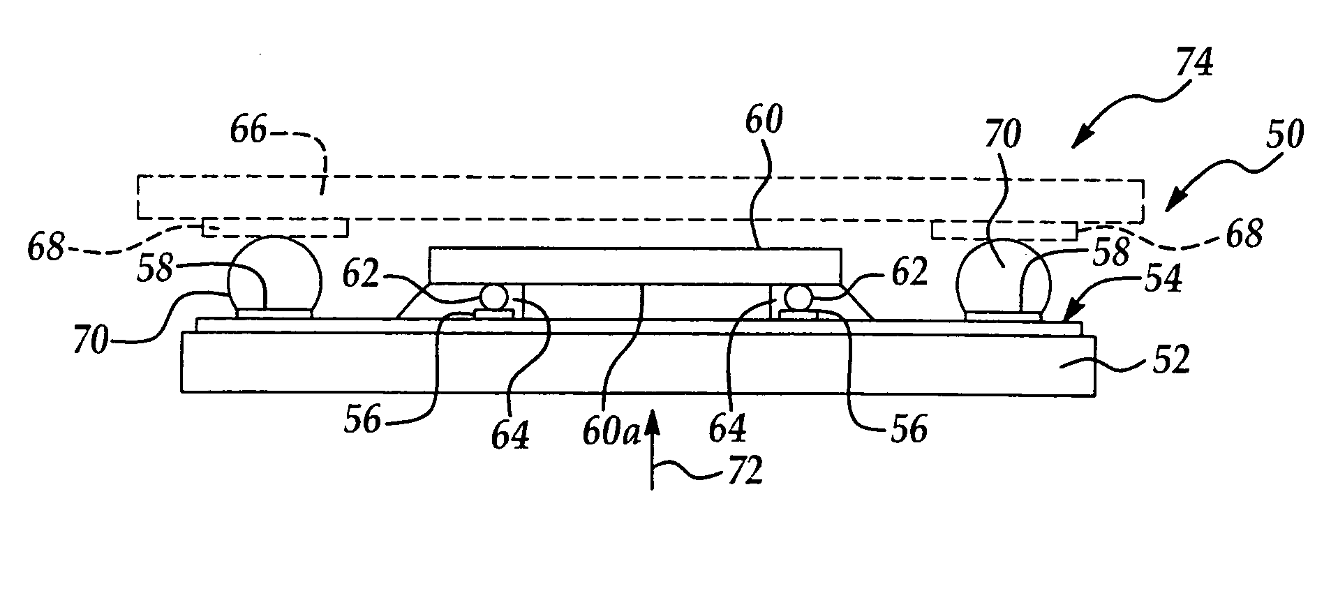
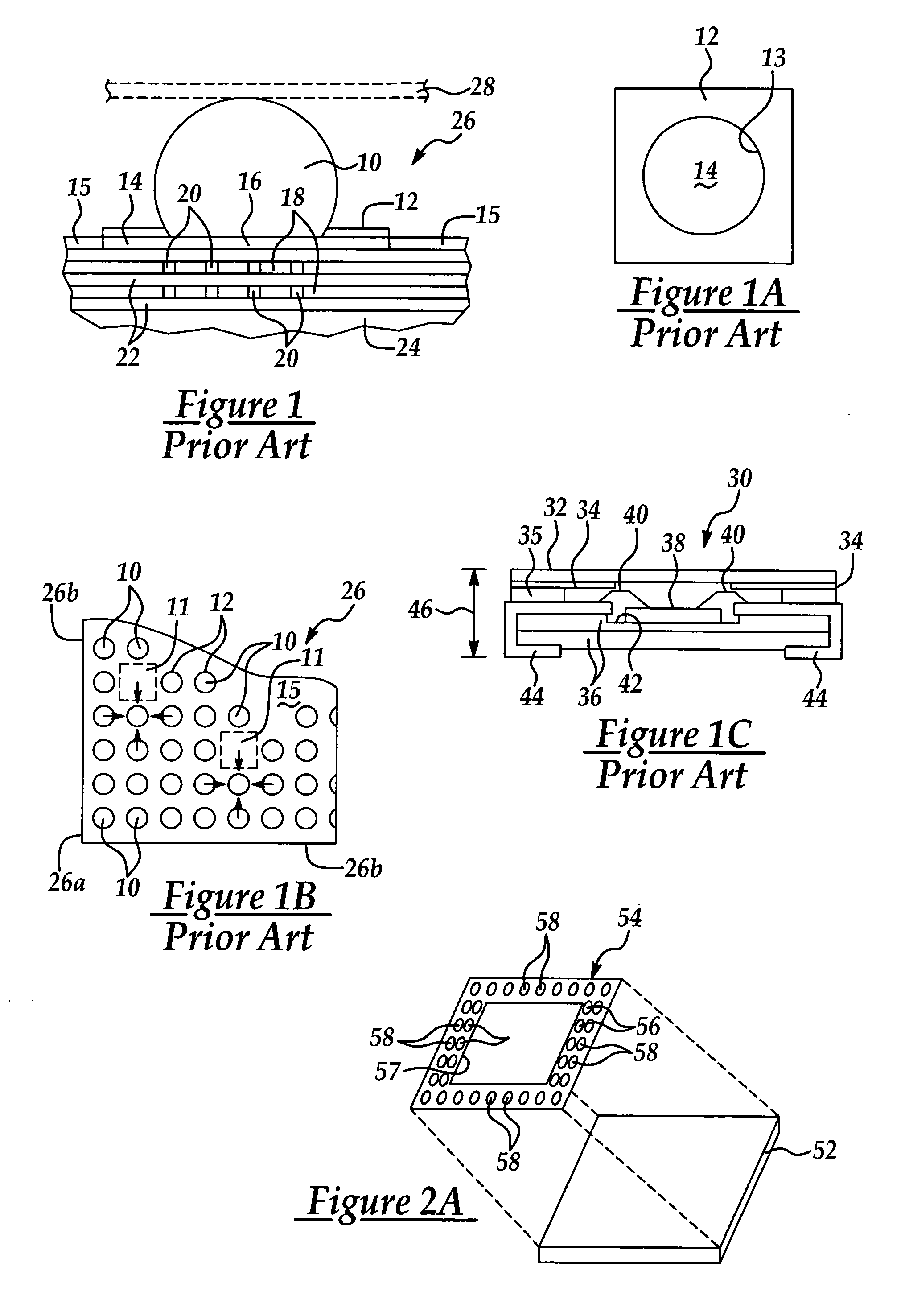
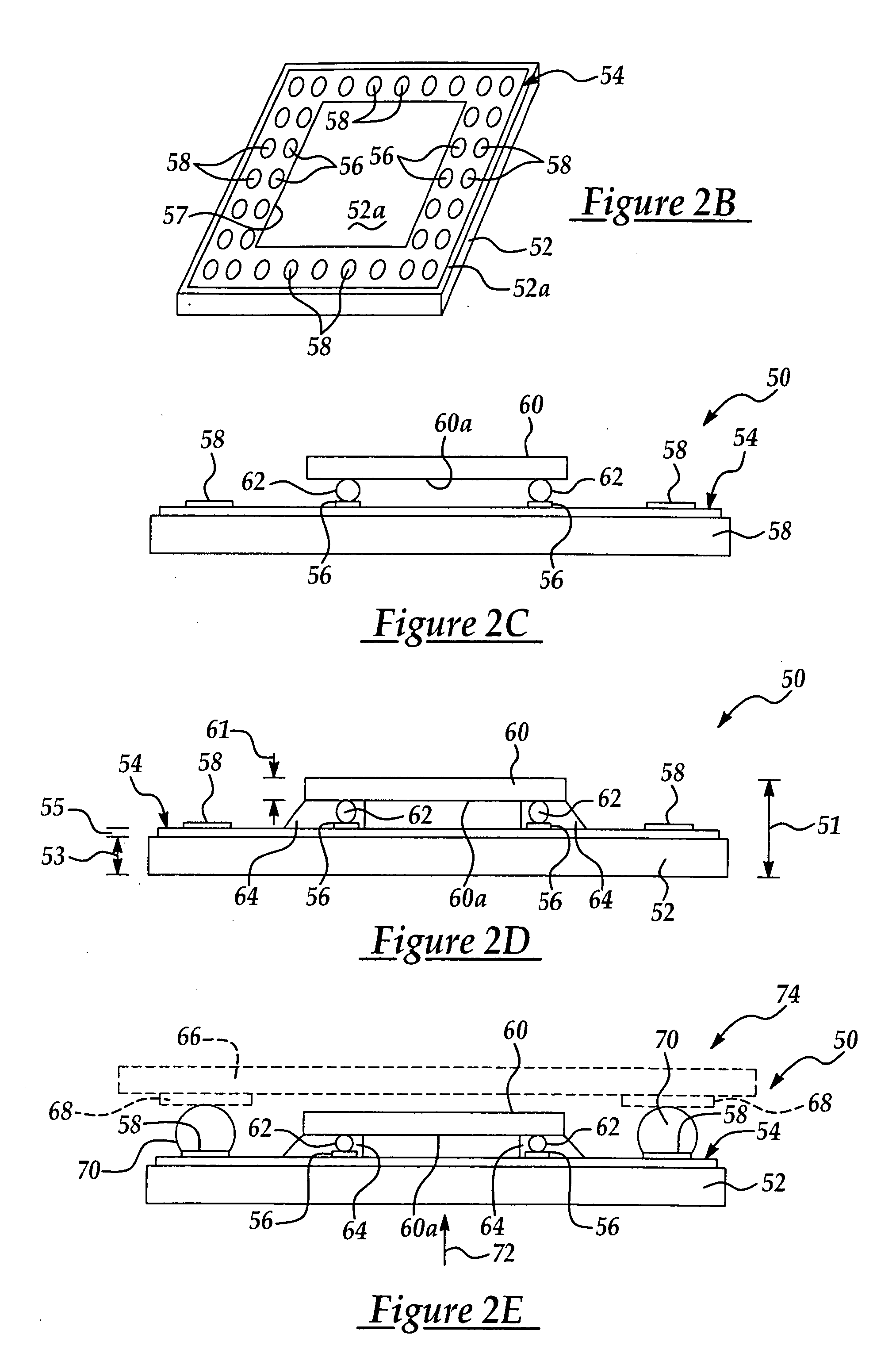
[0036] The present invention contemplates a structure and method for the packaging of an image sensor IC (integrated circuit) chip. The structure is a flip-chip BGA (ball grid array) packaging structure which is characterized by a high space efficiency as compared to conventional packaging structures for image sensors. Consequently, the image sensor device can be constructed in much smaller sizes than is possible using conventional packaging structures. The packaging structure may be adapted to either CCD image sensors or CMOS image sensors.

[0037] Referring initially to FIGS. 2D and 2E, a complete image sensor packaging structure 50 according to the present invention is shown. The packaging structure 50 includes a glass substrate 52, on which is provided a bond pad film 54 which is typically PI (polyimide) film, for example. As shown in FIG. 2D, the glass substrate 52 has a substrate thickness 53 of from typically about 400 μm to typically about 600 μm, whereas the bond pad film 54...


PUM


Abstract

A new and improved image sensor packaging structure and method. The image sensor packaging structure includes a glass substrate. A bond pad film, on which is provided multiple, interior flip-chip bond pads and exterior BGA (ball grid array) bond pads, is provided on the glass substrate. An inverted image sensor chip is bonded to the flip-chip bond pads on the glass substrate. The light-receiving face of the chip faces the glass substrate typically through a window provided in the bond pad film. Solder bumps are provided on the BGA bond pads on the bond pad film, and bond pads on a PCB (printed circuit board) are bonded to the respective solder bumps.

Description

FIELD OF THE INVENTION [0001] The present invention relates to flip chip packaging of semiconductor integrated circuits. More particularly, the present invention relates to a flip-chip packaging structure and method which reduces space particularly in the packaging of image sensors. BACKGROUND OF THE INVENTION [0002] One of the last processes in the production of semiconductor integrated circuits (IC) is multi-leveled packaging, which includes expanding the electrode pitch of the IC chips containing the circuits for subsequent levels of packaging; protecting the chip from package internal and external stress; providing proper thermal paths for channeling heat dissipated by the chip; and forming electronic interconnections. The manner in which the IC chips are packaged dictates the overall cost, performance, and reliability of the packaged chips, as well as of the system in which the package is applied. [0003] Package types for IC chips can be broadly classified into two groups: herm...

Claims


Application Information

Patent Timeline
IPC IPC(8): H01L21/00H01L27/146H01L31/0203
CPCH01L27/14618H01L31/0203H01L2924/10253H01L2224/16225H01L2924/30107H01L2224/24226H01L2224/32145H01L2224/48091H01L2224/48247H01L2924/01077H01L2924/01078H01L2924/19041H01L2924/00014H01L2924/00H01L2224/05085H01L2224/05571H01L2224/05001H01L2224/16238H01L24/05H01L24/16
Inventor CHEN, SHOU-LUNGLEU, FANG-JUNYU, SHAN-PU
Owner IND TECH RES INST
Why Eureka
Try Eureka