

Structure of image sensor module and a method for manufacturing of wafer level package
a technology of image sensor module and manufacturing method, which is applied in the direction of television system, radio frequency controlled devices, printed circuit non-printed electric components association, etc., can solve the problems of reducing yield, reducing package technology, and reducing the yield of frame package technology, so as to facilitate the final testing of wafer level package, reduce the cost of package structure, and increase the yield of package structure
- Summary
- Abstract
- Description
- Claims
- Application Information
AI Technical Summary
Benefits of technology
Problems solved by technology
Method used
Image

Examples
Embodiment Construction
[0024] Some sample embodiments of the invention will now be described in greater detail. Nevertheless, it should be recognized that the present invention can be practiced in a wide range of other embodiments besides those explicitly described, and the scope of the present invention is expressly not limited expect as specified in the accompanying claims.
[0025] Then, the components of the different elements are not shown to scale. Some dimensions of the related components are exaggerated and meaningless portions are not drawn to provide a more clear description and comprehension of the present invention.
[0026] The die of the present invention may be packaged with passive components (ex. capacitors) or other dies with a side by side structure or a stacking structure. The IC package can be finished by semiconductor industry and LCD industry.
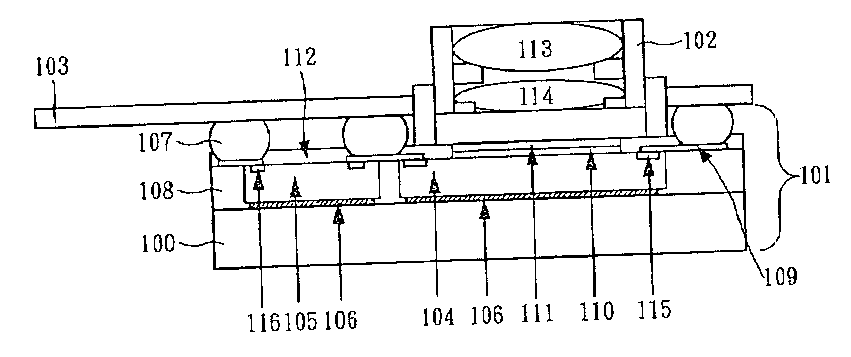
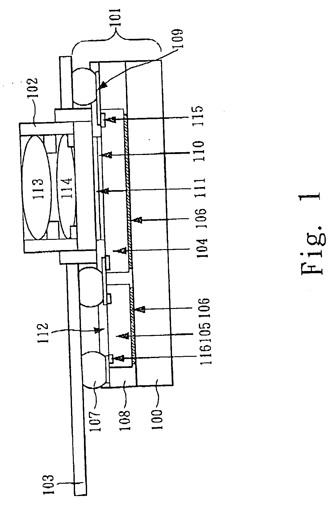
[0027] As aforementioned, the present invention provides an image sensor module, as shown in FIG. 1. The cross-section of the wafer level package...
PUM
 Abstract
Description
Claims
Application Information