Organic electroluminescence pixel circuit

a technology of electroluminescence and pixel circuit, applied in the field of organic electroluminescence, can solve the problems of reducing the aperture ratio, difficult to prevent the variation of the threshold value of switching the tfts on and off, and degrading the display quality, so as to achieve effective compensation

Active Publication Date: 2005-11-03
SANYO ELECTRIC CO LTD
View PDF2 Cites 62 Cited by
  • Summary
  • Abstract
  • Description
  • Claims
  • Application Information

AI Technical Summary

Benefits of technology

[0012] The present invention advantageously provides a pixel circuit which can effectively compensate for a variation in threshold voltages among driver transistors.
[0014] In addition, one terminal of a potential controlling transistor is connected to an emission set line. Because a voltage from a predetermined power supply is set on the emission set line, the voltage on the emission set line is stable, basically without being affected by factors such as the current flowing through the organic EL element. It is therefore possible to accurately set the voltage on the control terminal of the driver transistor.

Problems solved by technology

In this pixel circuit, when the threshold voltages of the driver TFTs in the pixel circuits arranged in a matrix form vary, the brightness varies, and as a result, there is a problem that the display quality is degraded.
However, the characteristics of the TFTs in the pixel circuits over the entire display panel cannot be made identical to each other, and it is therefore difficult to prevent variation in the threshold values for switching the TFTs on and off.
Therefore, when these circuits are used, the number of elements in the pixel circuit is increased, resulting in a problem that the aperture ratio is reduced.
In addition, when a circuit for compensation is added, there is a problem that the peripheral circuit for driving the pixel circuit must also be changed.

Method used


Image

  • Organic electroluminescence pixel circuit
  • Organic electroluminescence pixel circuit
  • Organic electroluminescence pixel circuit

Examples


first alternative embodiment

(A) First Alternative Embodiment

[0081]FIG. 11 shows a structure according to a first alternative embodiment of the present invention. In the first alternative embodiment, a p-channel transistor is employed for the selection transistor T1 and the short-circuiting transistor T3 and an n-channel transistor is employed as the potential controlling transistor T2. In this configuration, an operation similar to the above-described embodiment is enabled by inverting the H level and the L level of the gate line GL from the levels of the gate line GL in the above-described embodiment.

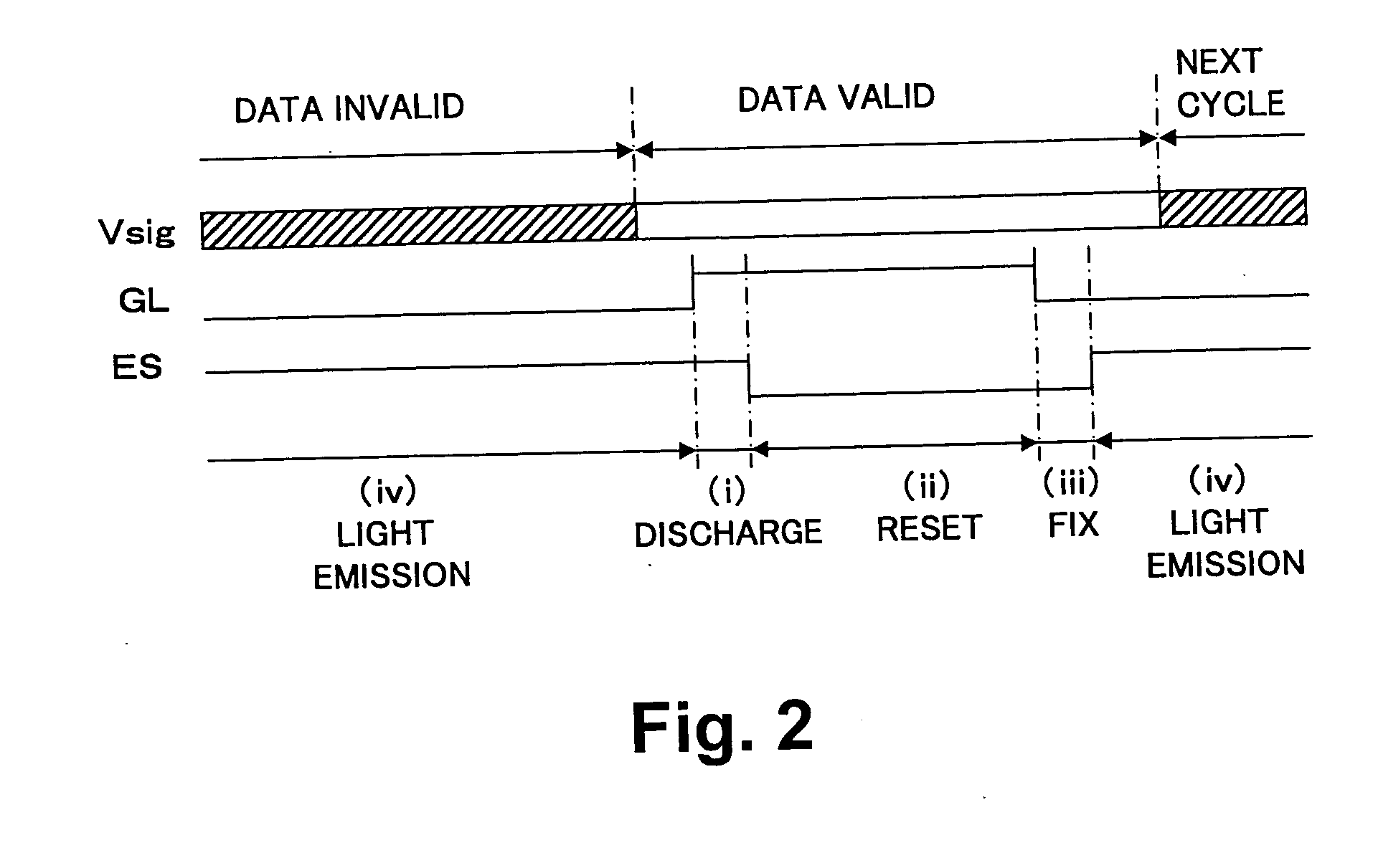
[0082] The on / off states of the selection transistor T1 and the drive controlling transistor T5 according to the control of the gate line GL and the emission set line ES are shown in FIG. 12, and are identical to those shown in FIG. 2.

second alternative embodiment

(B) Second Alternative Embodiment

[0083]FIG. 13 shows a structure according to a second alternative embodiment of the present invention. In the second alternative embodiment, a dedicated control line CS is additionally provided for controlling the potential controlling transistor T2, compared to the pixel circuit of the above-described embodiment. Therefore, it is possible to independently control the potential controlling transistor T2 using the control line CS. As shown in FIG. 14, with the control line CS, it is possible to switch the potential controlling transistor T2 off before the selection transistor T1 is switched on and to switch the potential controlling transistor T2 on along with the drive controlling transistor T5 after the selection transistor T1 is switched off.

[0084] In this configuration, although a number of lines along the horizontal direction is increased, it is possible to switch the potential controlling transistor T2 on and off at an optimum timing. In other ...

third alternative embodiment

(C) Third Alternative Embodiment

[0086]FIG. 18 shows another alternative embodiment of the present invention in which the selection transistor T1 and the potential controlling transistor T2 are connected to the gate line GL, a dedicated reset line RST is provided, and the short-circuiting transistor T3 is connected to the reset line RST. In this configuration, as shown in FIG. 19, the short-circuiting transistor T3 can be switched off using the reset line RST before the selection transistor T1 is switched off and the drive controlling transistor T5 is switched on.

[0087] Therefore, similar to the second alternative embodiment, it is possible to eliminate the period in which the potential controlling transistor T2 and the short-circuiting transistor T3 are simultaneously in the on state. With this structure, only two transistors, one being the selection transistor T1 and the other being the potential controlling transistor T2, need be provided near the gate line GL, which allows for e...


PUM


Abstract

A potential on a control terminal of a driver transistor is controlled and a drive current corresponding to the potential is supplied to an organic electroluminescence element. A drive controlling transistor is inserted between the driver transistor and the organic electroluminescence element and the drive current is switched on and off by the drive controlling transistor. A short-circuiting transistor is provided which controls whether or not the driver transistor is to be diode-connected. A selection transistor controls whether or not a data signal from a data line is to be supplied to the control terminal of the driver transistor. A capacitor is placed between the selection transistor and the control terminal of the driver transistor and a connection between a terminal of the capacitor on the side of the selection transistor and a predetermined power supply is switched on and off by a potential controlling transistor.

Description

CROSS-REFERENCE TO RELATED APPLICATIONS [0001] The entire disclosure of Japanese Patent Application Nos. 2004-117332, 2005-92566, 2005-92588, and 2005-96835 including specification, claims, drawings and abstract is incorporated herein by reference. BACKGROUND OF THE INVENTION [0002] 1. Field of the Invention [0003] The present invention relates to an organic electroluminescence (hereinafter simply referred to as “EL”) pixel circuit, which controls a drive current to be supplied to an organic EL element based on a data signal. [0004] 2. Description of the Related Art [0005] Because electroluminescence display devices wherein an EL element which is a self-emitting element is used as an emissive element in each pixel have advantages such as the fact that the device is self-emitting, that the thickness can be reduced, and that the power consumption is small, they have attracted much attention as display devices offering alternatives to display devices such as liquid crystal display (LCD...

Claims


Application Information

Patent Timeline
Patent Type & Authority Applications(United States)
IPC IPC(8): G09F9/30G09G3/30G09G3/32H05B33/02H05B44/00
CPCG09G3/3233G09G2300/0819G09G2320/043G09G2300/0861G09G2300/0842G09G3/30
Inventor IKEDA, KYOJI
Owner SANYO ELECTRIC CO LTD
Why Eureka
Try Eureka