Thin imaging apparatus, a thin camera, and an imaging method

a thin camera and imaging apparatus technology, applied in the field of thin camera and imaging apparatus, can solve the problems of reducing yield, increasing process cost, and reducing resolution relative to the size of formed images, and achieve the effect of low profile and high quality image information

Active Publication Date: 2005-11-03
PANASONIC CORP
View PDF3 Cites 21 Cited by
  • Summary
  • Abstract
  • Description
  • Claims
  • Application Information

AI Technical Summary

Benefits of technology

[0016] To solve the foregoing problem, an object of the present invention is to provide a thin imaging apparatus having an extremely low profile whereby high quality image information can still be achieved with outstanding resolution.
[0021] The thickness of the optical system is at most approximately the thickness of the light guide in a thin imaging apparatus according to the present invention, thus affording an extremely low profile, while the optical distance from the incidence mirror through the light guide to the imaging device can be increased by simply increasing the length of the light guide. Our invention thus affords a low profile collector optics system with a long focal length. It is therefore not necessary to reduce the size of the subject image even though the imaging apparatus is extremely thin. An expensive imaging device in which the pixel pitch is reduced proportionally to the focal length such as required in a conventional low profile imaging apparatus is therefore not needed, and high resolution images can be captured.

Problems solved by technology

The size of the images formed by this lens thus becomes smaller in proportion to the focal length, resulting in a drop in resolution relative to the size of the formed image if the pixel pitch of the imaging device remains the same.
Increasing the resolution of the manufacturing process increases the process cost while also significantly reducing yield.
Increased device cost is thus unavoidable.
Furthermore, reducing the pixel pitch of the imaging device results in a drop in the light-receiving area of each pixel proportional to the square of the reduction rate of the pitch.
Additional space is also needed outside the light-receiving area of each pixel to provide a matrix of lines for driving each pixel of the imaging device and charge transfer lines in a CCD, for example, and reducing the pixel pitch thus also reduces the effective aperture ratio enabling light detection.
Light reception thus drops significantly, sufficient photoelectric conversion power is difficult to achieve, and image quality thus drops significantly.
Furthermore, the wavelength of visible light ranges from 200 nm to 800 nm, and the optical lens system becomes unable to resolve images at the wavelength level due to the diffraction limit.
Even if an imaging device with a higher pixel pitch is achieved at the expense of yield, cost, and photoelectric conversion power, there is a limit to how much the size and thickness of the imaging apparatus can be reduced by reducing the focal length of the lens while maintaining high resolution due to the diffraction limit of light.
An optical system having a total length greater than the required focal length is therefore needed in a conventional imaging apparatus, and reducing the size and thickness of the imaging apparatus is thus even more difficult.
More succinctly, there is a limit to the reduction in size and thickness that can be achieved by shortening the focal length of the lens system in a conventional arrangement, and reducing the thickness (profile) is exceedingly difficult because of the difficulty in shortening the distance between the imaging device and lens, which is dependent upon the focal length of the lens.

Method used


Image

  • Thin imaging apparatus, a thin camera, and an imaging method
  • Thin imaging apparatus, a thin camera, and an imaging method
  • Thin imaging apparatus, a thin camera, and an imaging method

Examples


embodiment 1

[0048] (Embodiment 1)

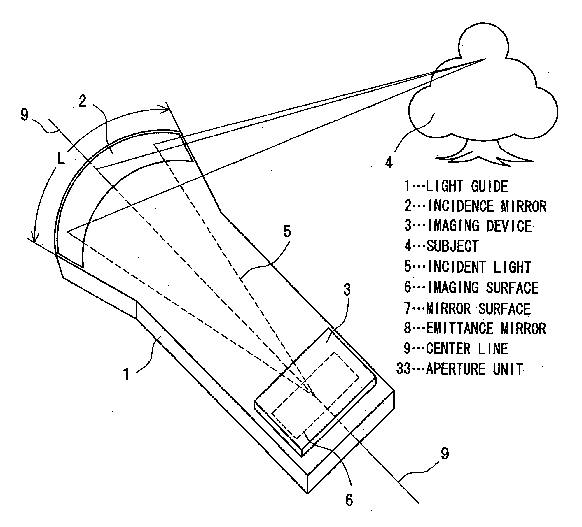
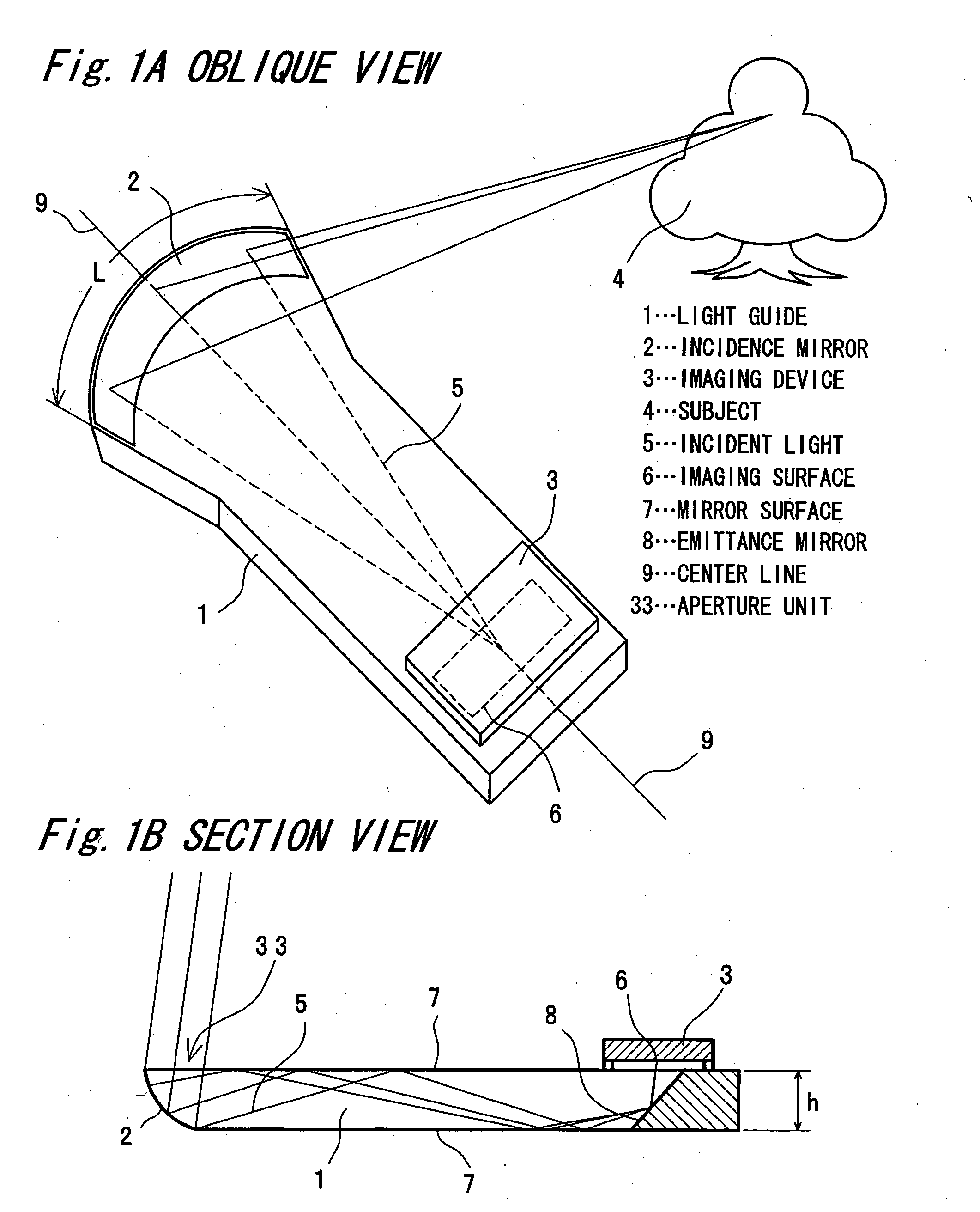
[0049] The arrangement of a thin imaging device according to a first embodiment of the present invention is described below with reference to FIGS. 1A and 1B. FIG. 1A is an oblique view of this thin imaging apparatus, and FIG. 1B is a section view through center line 9 in FIG. 1A.

[0050] As shown in FIGS. 1A and 1B this imaging apparatus has a light guide 1, incidence mirror 2, imaging device 3, emittance mirror 8, and aperture unit 33. The incidence mirror 2 is disposed at one end of the light guide 1, and the emittance mirror 8 and imaging device 3 are disposed at the other end of the light guide 1.

[0051] Light from the subject 4 passes through the aperture unit 33 and is incident to the imaging apparatus, reflected by the incidence mirror 2, and thus guided into the light guide 1. The incident light 5 thus guided forms an image on the imaging surface 6 of the imaging device 3, and the subject is thus imaged. The light guide 1 is a path through which the inci...

embodiment 2

[0074] (Embodiment 2)

[0075]FIGS. 5A and 5B show an optical arrangement in front of the imaging device 3 in a thin imaging apparatus according to a second embodiment of the present invention for selecting and separating incident light 5 according to the incidence angle. The arrangement whereby incident light 5 entering the light guide 1 reaches the front of the imaging device 3 is the same as described in the foregoing first embodiment of the invention.

[0076] Referring to FIG. 5A, an optical slit array 20 having slit portions 20a and shield portions 20b is disposed separated a specific distance from the front of the imaging surface 6 of the imaging device 3. Incident light 5a and 5b entering at different incidence angles therefore cast shadows at different positions on the imaging surface 6, and images from different incidence angles can thus be separated.

[0077] Because light obviously does not pass at the portions blocked by the shield portions 20b, the optical slit array 20 can b...

embodiment 3

[0080] (Embodiment 3)

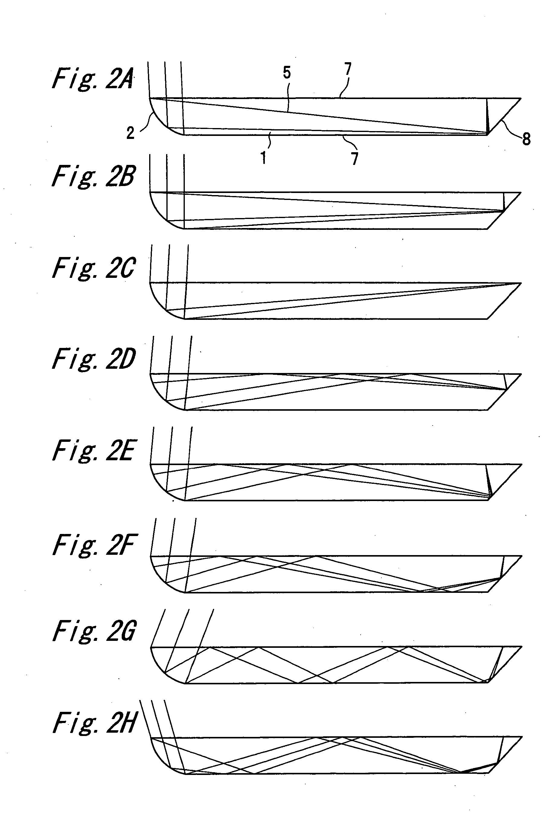
[0081]FIGS. 6A, 6B, and, 6C are section views showing a thin imaging apparatus according to a third embodiment of the present invention. As shown in FIG. 6A, the arrangement whereby light from the subject is reflected and guided by the incidence mirror 2 into the light guide 1 and then reflected by mirror surfaces 7 rendered on both main sides of the light guide 1 is the same as described in the foregoing first embodiment. This embodiment differs from the first embodiment, however, in that the emittance mirror 8 disposed in the first embodiment is not provided in this embodiment, and incident light guided to the end of the light guide 1 of imaging device side is received directly by the imaging device 3. The emittance mirror 8 in the first embodiment reflects the light to a main surface of the light guide 1 and thus makes disposing the imaging device 3 on the surface easier. Disposing the imaging device 3 as shown in FIG. 6A, however, affords both an extremely t...


PUM


Abstract

A thin imaging apparatus with an extremely low profile captures high quality images with outstanding resolution. The imaging apparatus has a light guide, incidence mirror, imaging device, and aperture unit. The incidence mirror reflects and guides light from a subject into the light guide, and the imaging device receives the light from the subject reflected by the incidence mirror and passing through the light guide.

Description

BACKGROUND OF THE INVENTION [0001] 1. Field of the Invention [0002] The present invention relates generally to an imaging apparatus such as a digital camera module, and relates more particularly to a thin imaging apparatus with an improved structure suitable for applications requiring an extremely thin profile such as in a portable information terminal. [0003] 2. Description of Related Art [0004] Reductions in the size and improvement in the performance of CCD, CMOS sensor, and other types of imaging devices combined with advanced optical technologies such as aspheric lenses have enabled downsizing the imaging apparatus in which these imaging devices are used. As a result, imaging apparatus are increasingly being used in highly portable devices that can be taken anywhere, including compact digital cameras and cell phones with a built-in camera. Anticipating a variety of situations, even greater compactness and thinness are desired in the camera modules used in such portable devices....

Claims


Application Information

Patent Timeline
Patent Type & Authority Applications(United States)
IPC IPC(8): G02B3/00G02B13/00G02B17/00G02B17/08G02B27/09
CPCG02B3/0043G02B3/005G02B13/0055H04N5/2254G02B17/08G02B17/086G02B27/0994G02B13/009H04N23/55
Inventor TOMITA, YOSHIHIROIMADA, KATSUMIKORENAGA, TSUGUHIRO
Owner PANASONIC CORP
Why Eureka
Try Eureka