Circuit device

a technology of circuit device and semiconductor element, applied in the direction of semiconductor/solid-state device testing/measurement, radiation controlled device, instruments, etc., can solve the problems of affecting the sealing resin, affecting the light signal, and affecting the light transmission performance, etc., to achieve accurate relative positions of semiconductor elements, excellent light transmittance, and accurate fixation

Active Publication Date: 2005-11-10
SEMICON COMPONENTS IND LLC
View PDF8 Cites 16 Cited by
  • Summary
  • Abstract
  • Description
  • Claims
  • Application Information

AI Technical Summary

Benefits of technology

[0033] With the circuit device of the present invention, the cover portion transmitting light emitted and received by the semiconductor element is provided in the top face of the casing. Accordingly, this semiconductor can be sealed while the light emitted and received by the semiconductor element is prevented from attenuating. Furthermore, when glass is employed for the cover portion, the aforementioned effect can be enhanced since glass is a material excellent in light transmittance.
[0034] Furthermore, the portion of the cover portion with a certain thickness on the bottom side is accommodated in the concave portion provided in the upper portion of the casing, and the position of the cover portion can be accurately fixed. Accordingly, it is possible to obtain accurate relative positions of the semiconductor element accommodated within the casing and the cover portion.
[0035] Furthermore, the communication portion allowing the internal space and the outside to communicate with each other is provided. Accordingly, it is possible to prevent the cover portion from being damaged by changes in pressure inside the casing due to temperature variations in use.
[0036] With the circuit device of the present invention, the plurality of portions exposed to the inside of the casing are provided for one lead, and the incorporated circuit elements can be electrically connected to each other by this lead. This can simplify a pattern of a mounting board on which the circuit device is to be mounted. Furthermore, according to the present invention, the plurality of portions exposed to the outside of the casing can be formed in one lead, and, therefore, the aforementioned effect can be further enhanced.
[0037] Still furthermore, the plurality of portions exposed to the inside of the casing are provided for one lead, and the circuit element is fixed to the exposed portions through the solder material. Accordingly, this solder material can be prevented from unnecessarily spreading.
[0038] The circuit device of the present invention includes the communication portion allowing the internal space of the casing and the outside to communicate with each other. This can prevent reduction of reliability due to dew condensation of moisture contained in gas staying in the internal space of the casing. Furthermore, this communication portion is formed in the area where the semiconductor element is arranged. Accordingly, the communication portion can be formed without increasing the size of the entire device.

Problems solved by technology

However, in the case where an element emitting and receiving short-wavelength light is employed as the aforementioned semiconductor device 104, many problems are caused.
Specifically, such problems include a case where short-wavelength light adversely affects the sealing resin 103 and a case where a light signal is degraded by sealing resin.

Method used


Image

  • Circuit device
  • Circuit device
  • Circuit device

Examples


first embodiment

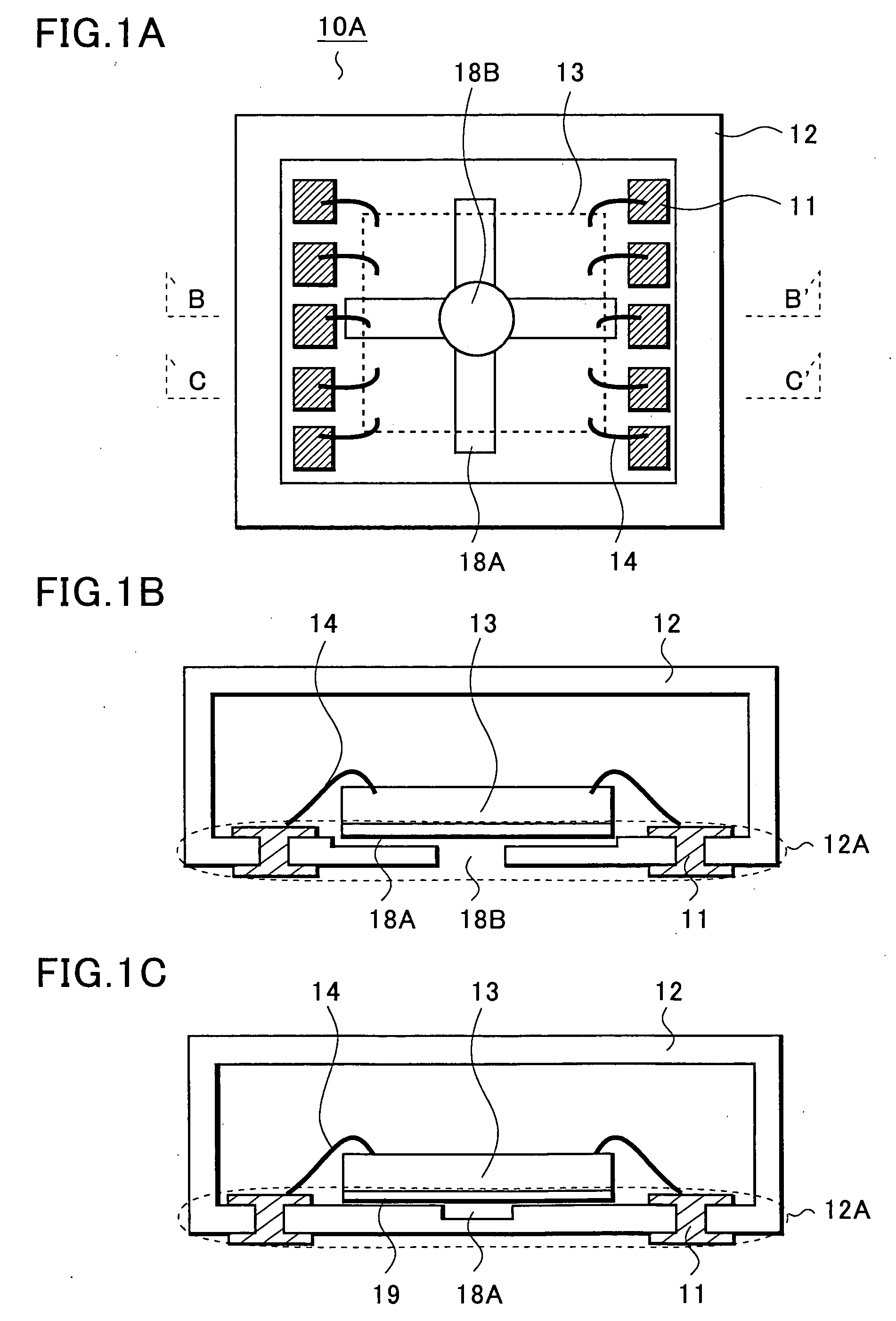
[0049] A description is given to a concrete configuration of a circuit device 10A according to an embodiment of the present invention with reference to FIGS. 1A to 1C. FIG. 1A is a plan view of the circuit device 10A, FIG. 1B is a cross-sectional view taken along a line B-B′ of FIG. 1A, and FIG. 1C is a cross-sectional view taken along a line C-C′ of FIG. 1A.

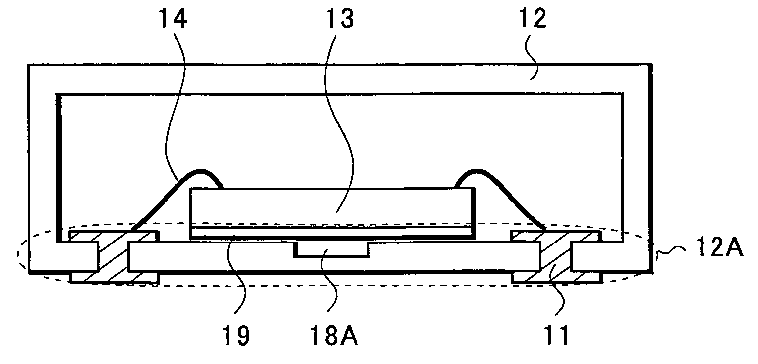
[0050] The circuit device 10A of the preferred embodiment includes a casing 12, a semiconductor element 13, a communication portion, and leads 11. The semiconductor element 13 is arranged in a bottom portion 12A of a casing 12. The communication portion is provided in a portion of the bottom portion 12A corresponding to an area where the semiconductor element 13 is arranged. The communication portion allows the inside of the casing 12 and the outside to communicate with each other. The leads 11 are electrically connected to the semiconductor element 13 and extended to the outside of the casing 12.

[0051] The casing 12 has a hol...

second embodiment

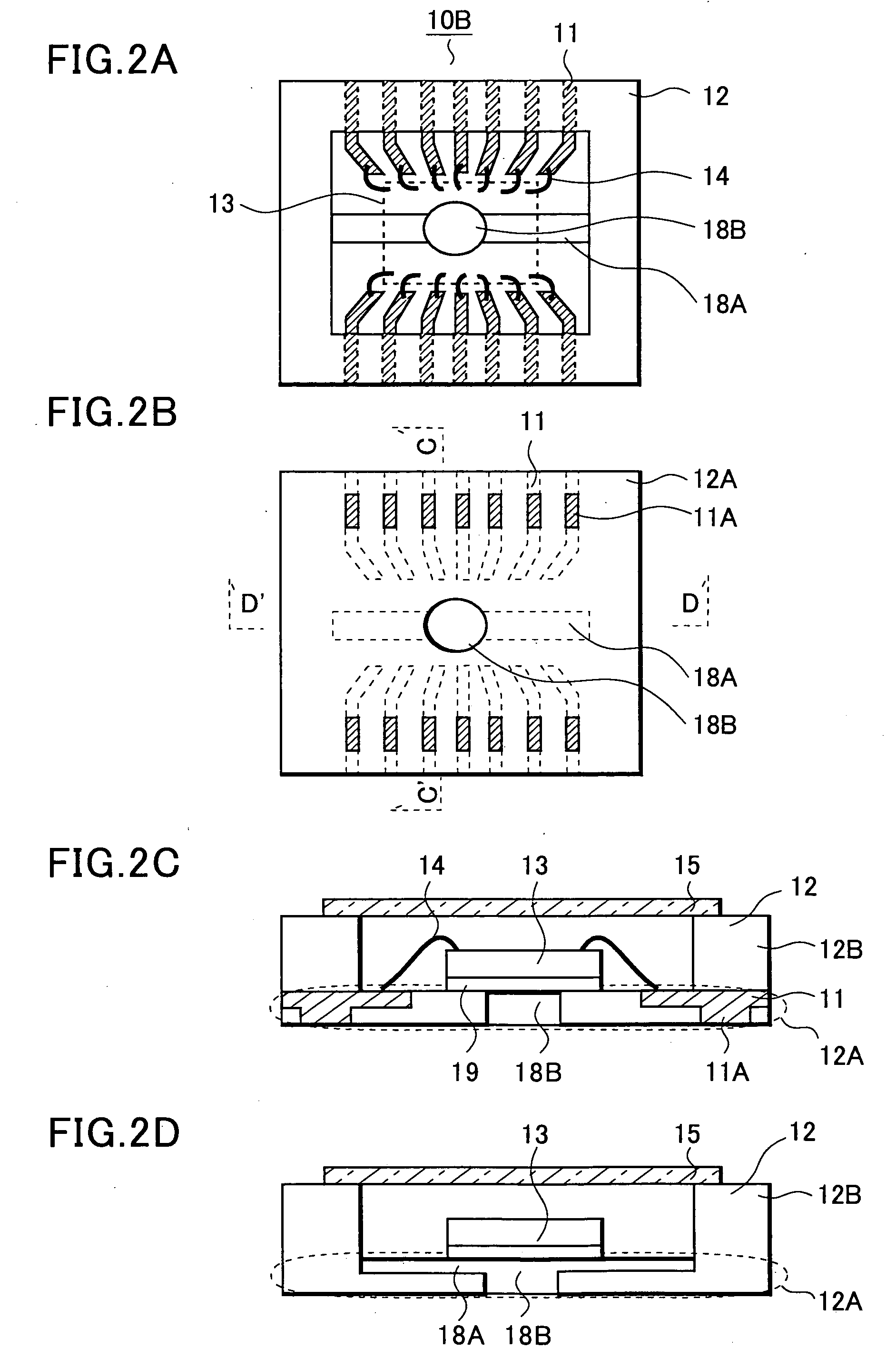
[0072] A concrete configuration of a circuit device 10 according to an embodiment of the present invention is described with reference to FIGS. 3A to 3C. FIG. 3A is a plan view of the circuit device 10, FIG. 3B is a cross-sectional view taken along a line B-B′ of FIG. 3A, and FIG. 3C is an enlarged cross-sectional view around the concave portion 25.

[0073] The circuit device 10 of this embodiment includes a casing 12, a semiconductor element 13A, and a cover portion 15. The casing 12 has an opening in the top face. The semiconductor element 13A is incorporated in the casing 12 and emits or receives light. The cover portion 15 is made of a material transmitting light and covers the opening. A concave portion25 is provided in the periphery of the opening portion and is configured to accommodate a portion of the cover portion 15 with a certain thickness on the bottom side. The structure of the thus structured circuit device 10 is described in detail below.

[0074] The casing 12 includes...


PUM


Abstract

To provide a circuit device suitable for incorporating a semiconductor element emitting or receiving short-wavelength light. The circuit device includes a casing, a semiconductor element, and a cover portion. The casing has an opening on the top face thereof. The semiconductor element is incorporated in the casing and emits or receives light. The cover portion is made of a material transparent to the light and covers the opening. In the periphery of the opening, a concave portion is provided, and a portion of the cover portion with a certain thickness on the bottom side is accommodated in the concave portion. Since the portion of the cover portion with the certain thickness on the bottom side is accommodated in the concave portion provided in the upper portion of the casing, the position of the cover portion is accurately fixed. Accordingly, it is possible to obtain accurate relative positions of the semiconductor element accommodated within the casing and the cover portion.

Description

[0001] Priority is claimed to Japanese Patent Application Number JP2004-040883 filed on Feb. 18, 2004, the disclosure of which is incorporated herein by reference in its entirety. BACKGROUND OF THE INVENTION [0002] 1. Field of the Invention [0003] The present invention relates to a circuit device of a hollow structure with a semiconductor element housed in a casing thereof. [0004] 2. Description of the Related Art [0005] A description is given of a constitution of a conventional circuit device 100 with reference to FIGS. 10A and 10B. FIG. 10A is a plan view of the circuit device 100, and FIG. 10B is a cross-sectional view thereof (see Patent Literature 1). [0006] Referring to FIGS. 10A and 10B, a land 102 made of a conductive material is formed in the center of the circuit device 100, and around the land 102, one end of each of a number of leads 101 is in close vicinity thereof. The one end of each lead 101 is electrically connected to a semiconductor element 104 through a thin meta...

Claims


Application Information

Patent Timeline
Patent Type & Authority Applications(United States)
IPC IPC(8): H01L21/52H01L21/56H01L21/66H01L23/02H01L25/16H01L27/146H05K1/00H05K1/02H05K1/18
CPCH01L25/167H01L27/14618H01L2924/07802H01L2924/01029H01L2924/1815H01L2224/97H01L24/97H01L2924/3025H01L2924/19041H01L2224/73265H01L33/486H01L2224/48091H01L2224/48247H01L2924/00014H01L2224/85H01L2924/00H01L2924/12042H01L2924/14H01L2924/16195
Inventor INOGUCHI, HIROSHI
Owner SEMICON COMPONENTS IND LLC
Why Eureka
Try Eureka