Method of forming a top gate thin film transistor
a thin film transistor and top gate technology, applied in the field of thin film transistor (tft) process, can solve the problems of complicated and expensive traditional process, and achieve the effect of reducing cost and reducing reticle consumption
- Summary
- Abstract
- Description
- Claims
- Application Information
AI Technical Summary
Benefits of technology
Problems solved by technology
Method used
Image

Examples
first embodiment
[0022]FIGS. 2A-2H are sectional views showing the top gate TFT process according to the first embodiment of the present invention.
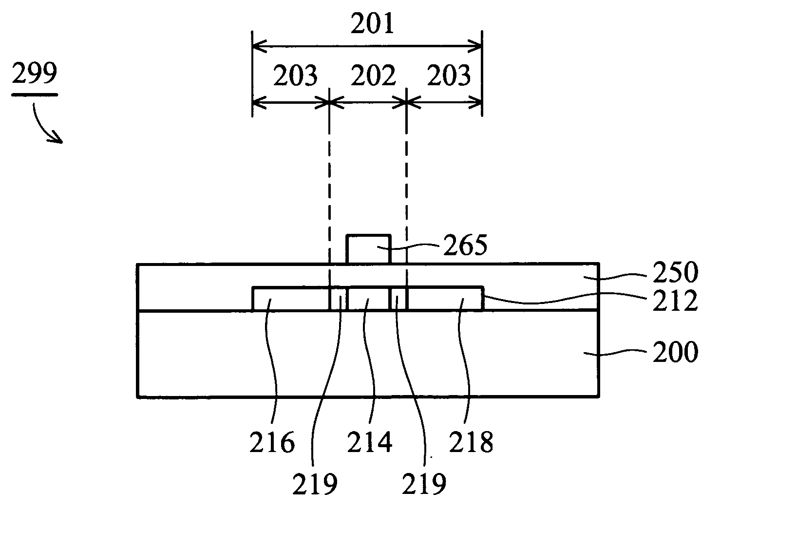
[0023] In FIG. 2A, a transparent insulating substrate 200 having at least one predetermined active area 201 thereon is provided, wherein the active area 201 includes a channel area 202 and a source / drain area 203. The transparent insulating substrate 200 can be a glass substrate. A silicon layer 210, such as amorphous silicon or polysilicon, is then formed on the substrate 200.
[0024] In FIGS. 2A and 2B, a positive photoresist layer 220 is formed on the silicon layer 210. By performing photolithography (patterning procedure) using a first reticle 230, a first photoresist layer 222 is formed on the silicon layer 210 in the active area 201, wherein the first photoresist layer 222 has a thick photoresist layer portion 224 and a thin photoresist layer portion 226, and the thin photoresist layer portion 226 corresponds to the channel area 202.
[0025] It shoul...
second embodiment
[0034]FIGS. 3A-3H are sectional views showing the top gate TFT process according to the second embodiment of the present invention.
[0035] In FIG. 3A, a transparent insulating substrate 300 having at least one predetermined active area 301 thereon is provided, wherein the active area 301 includes a channel area 302 and a source / drain area 303. The transparent insulating substrate 300 can be a glass substrate. Then, a silicon layer 310, such as amorphous silicon or polysilicon, is formed on the substrate 300.
[0036] In FIGS. 3A and 3B, a positive photoresist layer 320 is formed on the silicon layer 310. By performing photolithography (patterning procedure) using a first reticle 330, a first photoresist layer 322 is formed on the silicon layer 310 in the active area 301, wherein the first photoresist layer 322 has a thick photoresist layer portion 324 and a thin photoresist layer portion 326, and the thick photoresist layer portion 324 corresponds to the channel area 302.
[0037] It sh...
third embodiment
[0045]FIGS. 4A-4H are sectional views showing the top gate TFT process according to the third embodiment of the present invention.
[0046] In FIG. 4A, a transparent insulating substrate 400 having at least one predetermined active area 401 thereon is provided, wherein the active area 401 includes a channel area 402 and a source / drain area 403. The transparent insulating substrate 400 can be a glass substrate. A silicon layer 410, such as amorphous silicon or polysilicon, is then formed on the substrate 400. An insulating layer 420, such as SiO2, is formed on the silicon layer 420. A first metal layer 430, such as Al or Mo, is next formed on the insulating layer 420.
[0047] In FIGS. 4A and 4B, a positive photoresist layer 440 is formed on the first metal layer 430. By performing photolithography (patterning procedure) using a reticle 450, a first photoresist layer 442 is formed on the first metal layer 430 in the active area 401, wherein the first photoresist layer 442 has a thick pho...
PUM
 Abstract
Description
Claims
Application Information
 - R&D
- Intellectual Property
- Life Sciences
- Materials
- Tech Scout
- Unparalleled Data Quality
- Higher Quality Content
- 60% Fewer Hallucinations
Browse by: Latest US Patents, China's latest patents, Technical Efficacy Thesaurus, Application Domain, Technology Topic, Popular Technical Reports.
© 2025 PatSnap. All rights reserved.Legal|Privacy policy|Modern Slavery Act Transparency Statement|Sitemap|About US| Contact US: help@patsnap.com