Direct cooling of LEDs

a technology of leds and leds, applied in semiconductor devices for light sources, semiconductor/solid-state device details, lighting and heating apparatus, etc., can solve the problem of relative increase in optical flux, and achieve the effect of efficient removal of hea

Active Publication Date: 2005-11-17
SILICON VALLEY BANK
View PDF8 Cites 46 Cited by
  • Summary
  • Abstract
  • Description
  • Claims
  • Application Information

AI Technical Summary

Benefits of technology

[0012] The present invention provides a cooling system for semiconductor devices...

Problems solved by technology

In such case, because the optical output of the semiconductor device tends to increase with the decreased temperature of t...

Method used


Image

  • Direct cooling of LEDs
  • Direct cooling of LEDs
  • Direct cooling of LEDs

Examples


Embodiment Construction

[0037] Representative embodiments of the present invention are shown in FIGS. 4-13, wherein similar features share common reference numerals.

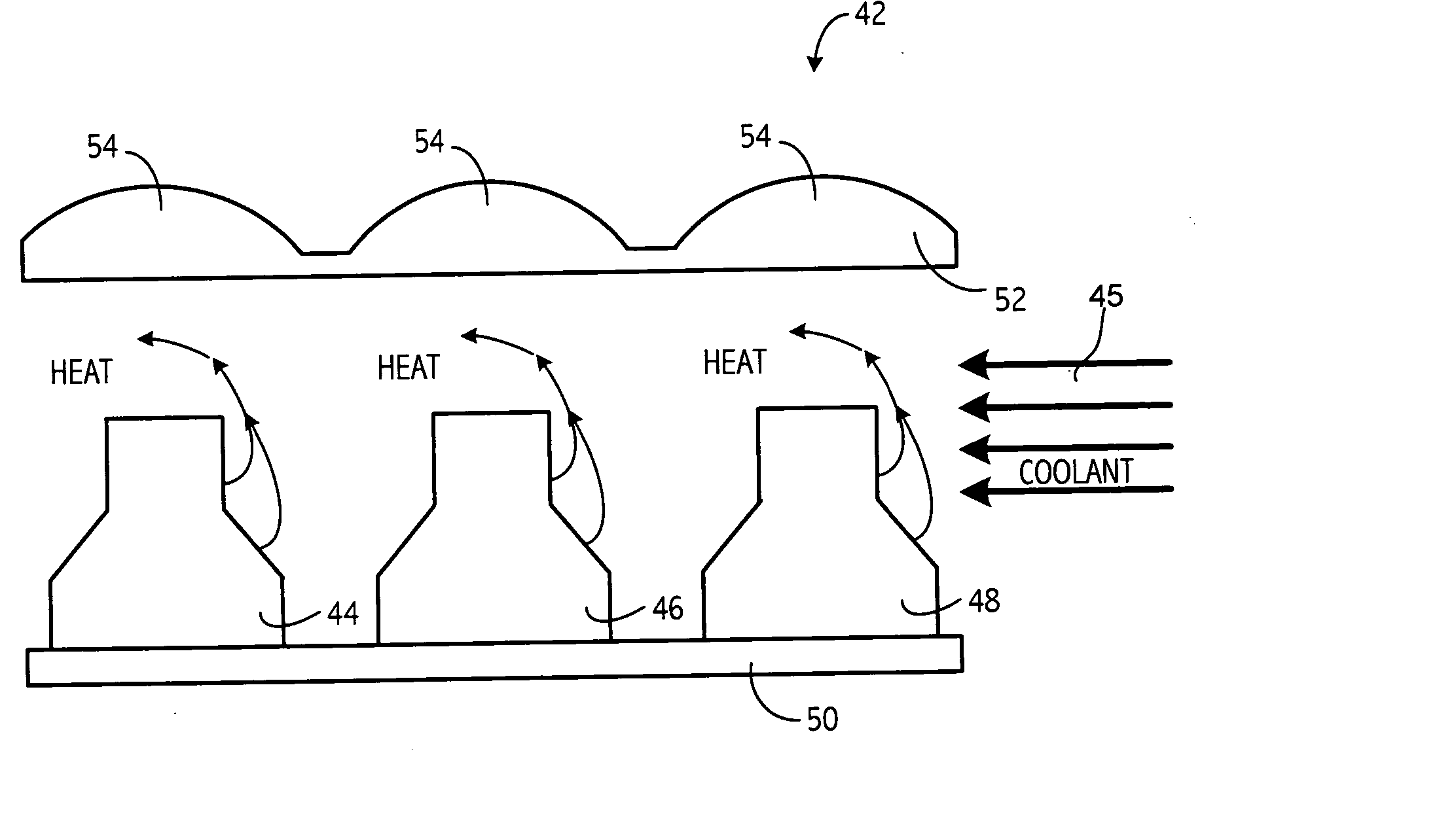
[0038]FIGS. 4-12 show examples of a semiconductor device such as a high-density LED array that may be used for applications requiring high optical power density at the working surface of a target material. In such applications, the target material is exposed with light for the purpose of illuminating or performing a material transformation in or of the target. Such applications may include, for example, curing applications ranging from ink printing to the fabrication of DVDs and lithography. One such high-density LED array is shown and described in U.S. patent application Ser. No. 10 / 984,589, filed Nov. 8, 2004, the entire contents of which are hereby incorporated by reference for all purposes. The invention is described for direct cooling of LEDs, preferably including the light-emissive surface of LEDs. However, the invention is not intende...


PUM


Abstract

A thermal management system is provided for semiconductor devices such as an LED array, wherein coolant directly cools the LED array. Preferably, the coolant may be selected, among other bases, based on its index of refraction relative to the index associated with the semiconductor device.

Description

RELATED APPLICATIONS [0001] This application claims priority from U.S. Provisional Application Ser. No. 60 / 554,632, filed Mar. 18, 2004, the contents of which are hereby incorporated by reference as if recited in full herein for all purposes.BACKGROUND OF THE INVENTION [0002] This invention relates to thermal management of semiconductor devices and, more particularly, to thermal management of semiconductor devices by direct cooling. [0003] Light-emitting diodes (LEDs) consist of a PN junction formed by two dissimilarly doped semiconductors as shown in FIG. 1. In this junction, one of the semiconductors (p) is doped so the majority carriers are positive (holes), while the other semiconductor (n) is doped so the majority carriers are negative (electrons). By applying an external electric field across the junction, current can be made to flow, and when the holes from the p-type and electrons from the n-type meet at the junction they combine and release a photon of light. [0004] The wav...

Claims


Application Information

Patent Timeline
IPC IPC(8): F21V29/02H01L23/34H01L23/473H01L25/075H01L33/64
CPCF21V29/30F21Y2101/02H01L23/473H01L25/0753H01L2924/0002H01L33/648H01L2924/00F21Y2115/10F21V29/59
Inventor OWEN, MARK D.VLACH, FRANCOISANDERSON, DUWAYNE R.
Owner SILICON VALLEY BANK
Why Eureka
Try Eureka