PWM controller having frequency jitter for power supplies

a power supply and controller technology, applied in the field of power supply, can solve the problems of power consumption, power converter size reduction, switching device generating electric and magnetic interference (emi) that interferes with the power source, etc., and achieve the effect of reducing the impedance of the attenuator, reducing the attenuation rate, and eliminating undesired ripple signals

Active Publication Date: 2005-11-17
SEMICON COMPONENTS IND LLC
View PDF16 Cites 34 Cited by
  • Summary
  • Abstract
  • Description
  • Claims
  • Application Information

AI Technical Summary

Benefits of technology

[0011] Both the first jitter current and the second jitter current are in triangle waveform. The switching frequency increases wherever the first jitter current increases, and vice versa. Therefore the switching frequency is modulated in response to the first jitter current. Meanwhile, the impedance of the attenuator decreases and the attenuation rate increases whenever the second jitter current increases. Therefore, the on-time of the switching signal is immediately reduced, which compensates the decrease of the switching period and keeps the output power as a constant. Since the on-time of the switching signal is feed-forward compensated in response to frequency jittering, undesired ripple signal can be eliminated.
[0012] Furthermore, the charge and the discharge of the triangle waveform are sliced enabled by the pulse signal. This can reduce the size of the modulator circuit.

Problems solved by technology

Although the switching technology reduces the size of the power converter, switching devices generate electric and magnetic interference (EMI) that interferes the power source.
However, the EMI filter 15 used to reduce the EMI causes power consumption and increases the cost and the size of the power supply.
However, the disadvantage of these prior arts is that the frequency jitter generates undesired ripple signal at the power supply outputs.

Method used


Image

  • PWM controller having frequency jitter for power supplies
  • PWM controller having frequency jitter for power supplies
  • PWM controller having frequency jitter for power supplies

Examples


Embodiment Construction

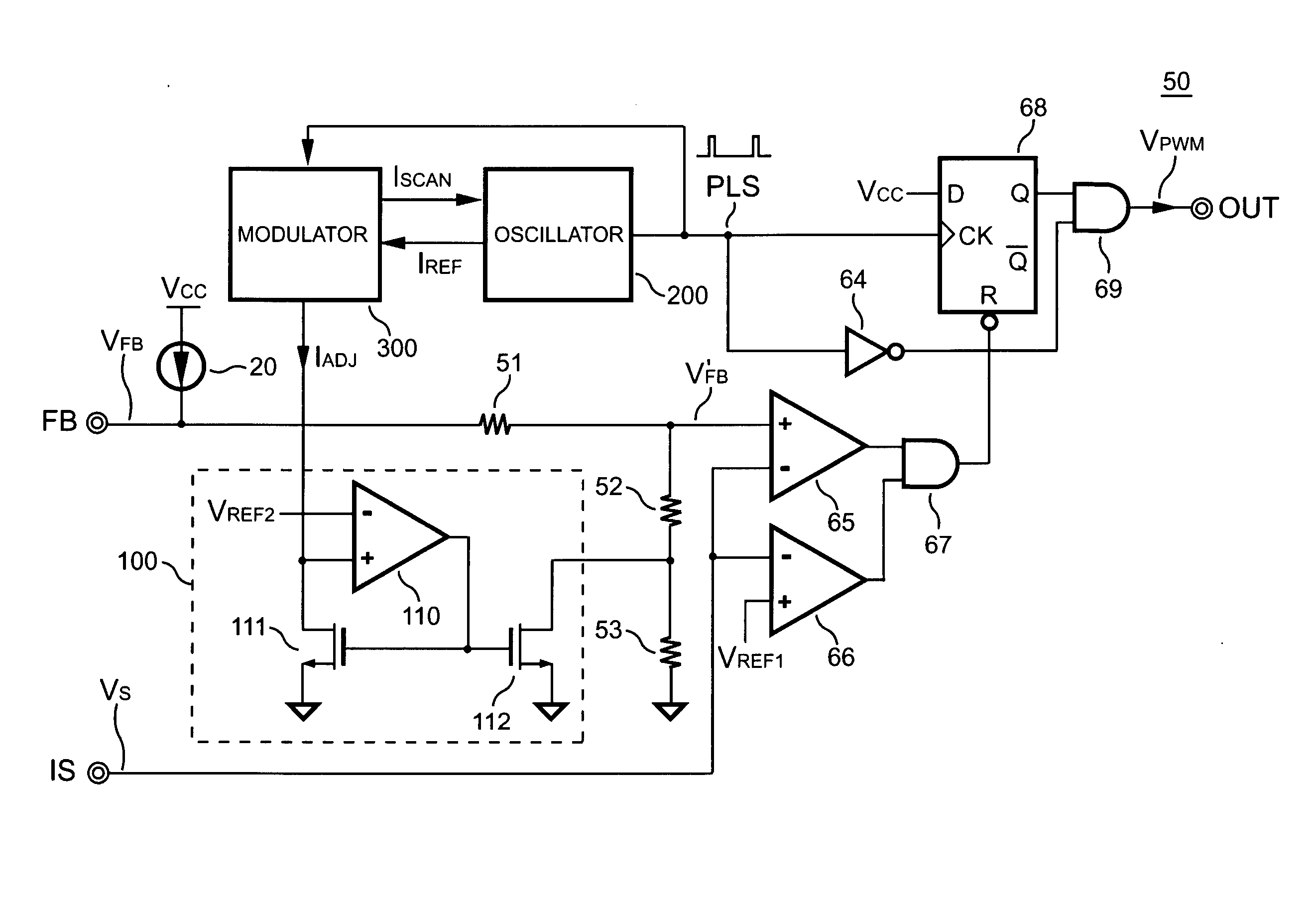
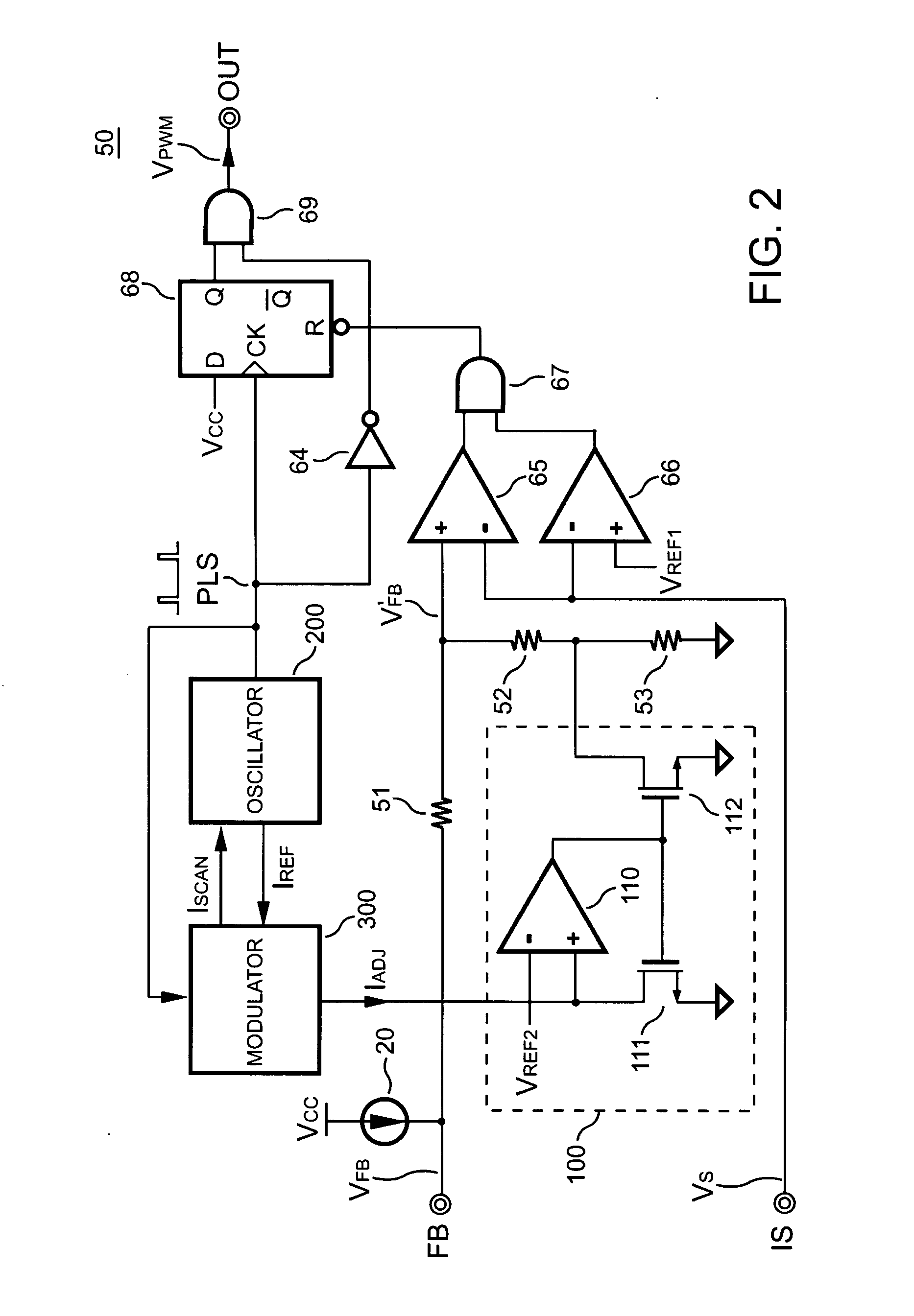
[0022]FIG. 2 is a circuit schematic of a PWM controller 50 having frequency jitter according to an embodiment of the present invention. The PWM controller 50 includes a modulator 300, an oscillator 200, a variable-resistance circuit 100, a first comparator 65 and a second comparator 66, a D flip-flop 68, an inverter 64, two AND gates 67, 69, and an attenuator formed by resistors 51, 52 and 53. In response to a pulse signal PLS and a reference current IREF generated by the oscillator 200, the modulator 300 generates a first jitter current ISCAN and a second jitter current IADJ. The first jitter current ISCAN is proportional to the second jitter current IADJ.

[0023] The first jitter current ISCAN and the second jitter current IADJ are in triangle waveform. The oscillator 200 generates the pulse signal PLS for determining a switching frequency in response to the modulation of the first jitter current ISCAN. The switching frequency increases whenever the first jitter current ISCAN incre...


PUM


Abstract

A PWM controller having frequency jitter includes a modulator for generating a first jitter current and a second jitter current. An oscillator generates a pulse signal for producing a switching frequency in response to the modulation of the first jitter current. An attenuator is connected in a voltage feedback loop for attenuating a feedback signal to an attenuated feedback signal, in which the attenuated feedback signal is utilized to control an on-time of a switching signal. A variable-resistance circuit is connected with the attenuator for programming an attenuation rate of the attenuator in response to the modulation of the second jitter current. The switching frequency increases whenever the first jitter current increases. Meanwhile, the impedance of the attenuator will decreases and the attenuation rate will increase whenever the second jitter current increase. The on-time of the switching signal is thus immediately reduced, which compensates the decrease of the switching period and keeps the output power as a constant.

Description

BACKGROUND OF THE INVNETION [0001] 1. Field of the Invention [0002] The present invention relates to a power supply and more specifically relates to PWM control of a switching mode power supply. [0003] 2. Description of Related Art [0004] Power supplies have been used to convert an unregulated power source to a regulated voltage or current. FIG. 1 shows a traditional power supply, in which a PWM controller 10 generates a switching signal for switching a transformer 11 via a transistor 20. The duty cycle of the switching signal determines the power delivered from an input of the power source to an output of the power supply. Although the switching technology reduces the size of the power converter, switching devices generate electric and magnetic interference (EMI) that interferes the power source. An EMI filter 15 equipped at an input of the power supply is utilized to resist the EMI into the input of the power source. However, the EMI filter 15 used to reduce the EMI causes power c...

Claims


Application Information

Patent Timeline
Patent Type & Authority Applications(United States)
IPC IPC(8): H02M3/335H03K3/017H03K3/0231H03K7/08H04B15/04
CPCH02M3/33507H03K3/0231H04B2215/067H04B15/04H04B2215/064H03K7/08
Inventor YANG, TA-YUNGHUNG, GUO-KIANGLIN, SONG-YI
Owner SEMICON COMPONENTS IND LLC
Why Eureka
Try Eureka