Power stack

a technology of power stack and cooling balance, applied in the direction of resistor details, electrical apparatus construction details, lighting and heating apparatus, etc., can solve the problems of power stack cooling balance, etc., to prevent the cooling efficiency from locally deteriorating and excellent cooling balance

Active Publication Date: 2005-11-24
DENSO CORP
View PDF12 Cites 81 Cited by
  • Summary
  • Abstract
  • Description
  • Claims
  • Application Information

AI Technical Summary

Benefits of technology

[0011] In view of the above-described problems, the present invention has an object to provide a power stack capable of reducing or eliminating local deterioration in the cooling efficiency and accordingly capable of assuring excellent cooling balance.

Problems solved by technology

However, the above-described prior art documents 1 to 4 disclose nothing about the layout of the semiconductor elements in the power stack.
Therefore, according to the power stacks disclosed in the prior art documents 1 to 4, the power stack will have bad cooling balance as a whole when the semiconductor elements have different heat generation rates.
If the layout of semiconductor elements is determined without considering differences of heat generation rates, the power stack will have undesirably deviated distribution of heat generation rates as a whole.
Having the undesirably deviated distribution of heat generation rates is not desirable because portions having higher cooling efficiencies and portions having lower cooling efficiencies appear locally in the power stack.
In short, the power stack as a whole has a bad cooling balance.
Accordingly, there will be a possibility that semiconductor elements cannot be sufficiently cooled in a case that the layout of semiconductor elements in the power stack is improper.

Method used


Image

  • Power stack
  • Power stack
  • Power stack

Examples


first embodiment

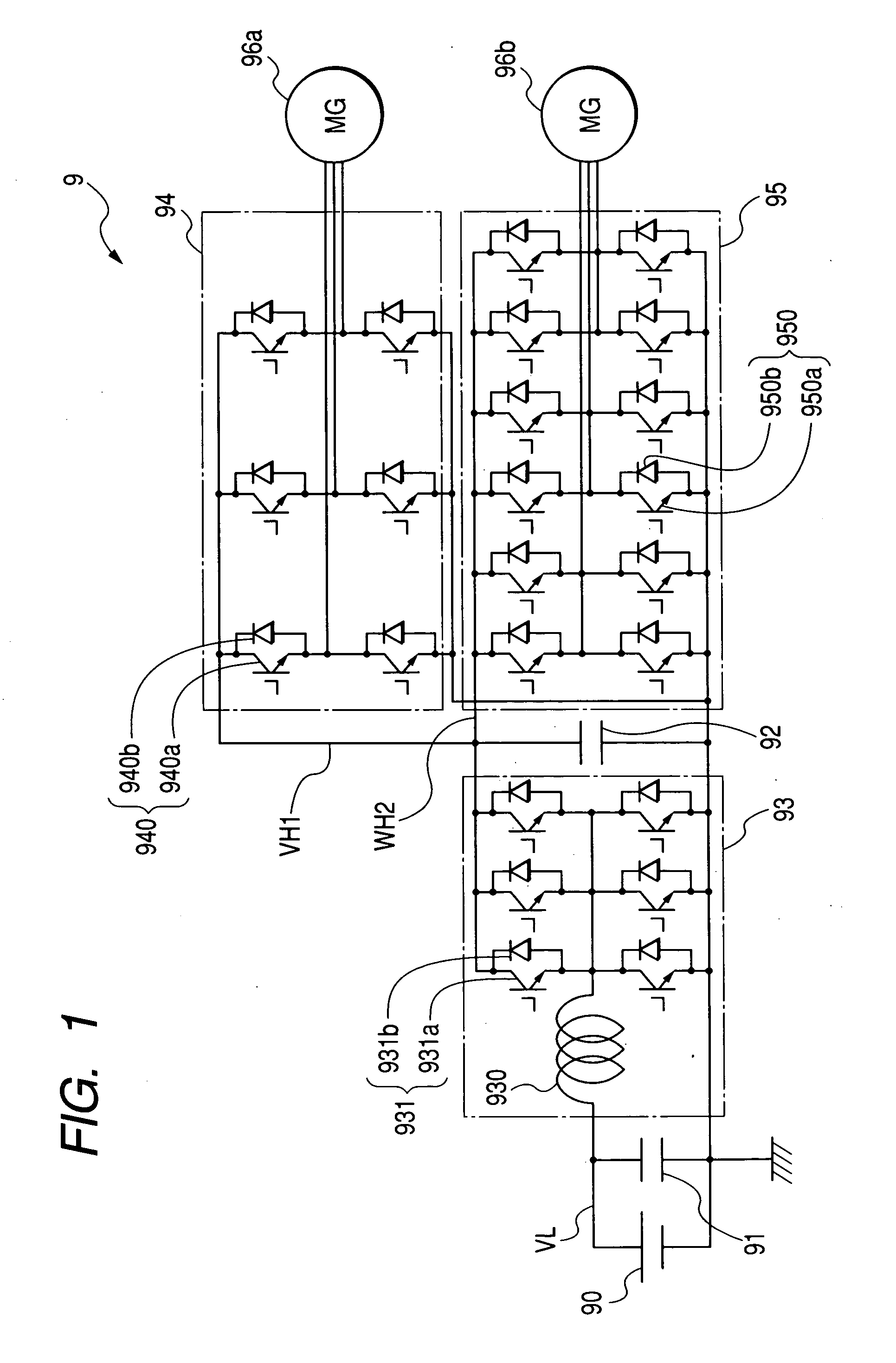
[0056] First, a driving apparatus for a MG (i.e. electric Motor / Generator) will be explained as an example using a power stack of this embodiment. FIG. 1 shows a circuit diagram of this driving apparatus. As shown in the drawing, a driving apparatus 9 includes a battery 90, smoothing capacitors 91 and 92, a DC-DC converter 93, a first inverter circuit 94, and a second inverter circuit 95.

[0057] The DC-DC converter 93 includes an electric reactor 930 and a plurality of converter switching modules 931. One end of the electric reactor 930 is connected to a connecting point of high-potential side converter switching modules 931 and low-potential side converter switching modules 931 which are later described in more detail. The other end of the electric reactor 930 is connected to a high-voltage terminal of the battery 90 via a low-voltage power line VL.

[0058] Each converter switching module 931 consists of an IGBT (i.e. Insulated Gate Bipolar Transistor) 931a and a flywheel diode 931b...

second embodiment

[0091] The second embodiment is different from the first embodiment in that the electric reactor 930 and the converter switching module 931 shown in FIG. 1 are disposed in the power stack. Hereinafter, this embodiment is explained only about the differences.

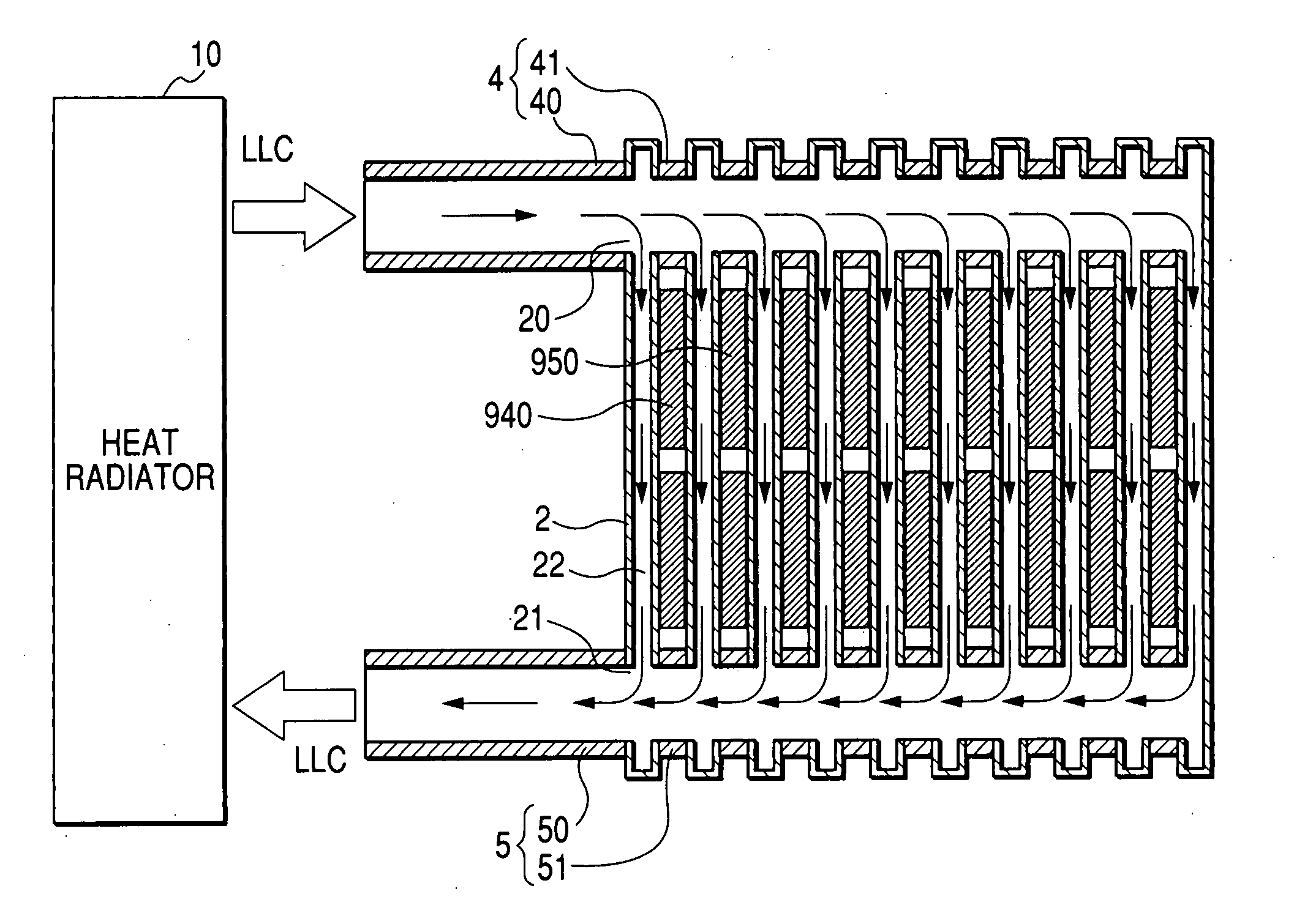
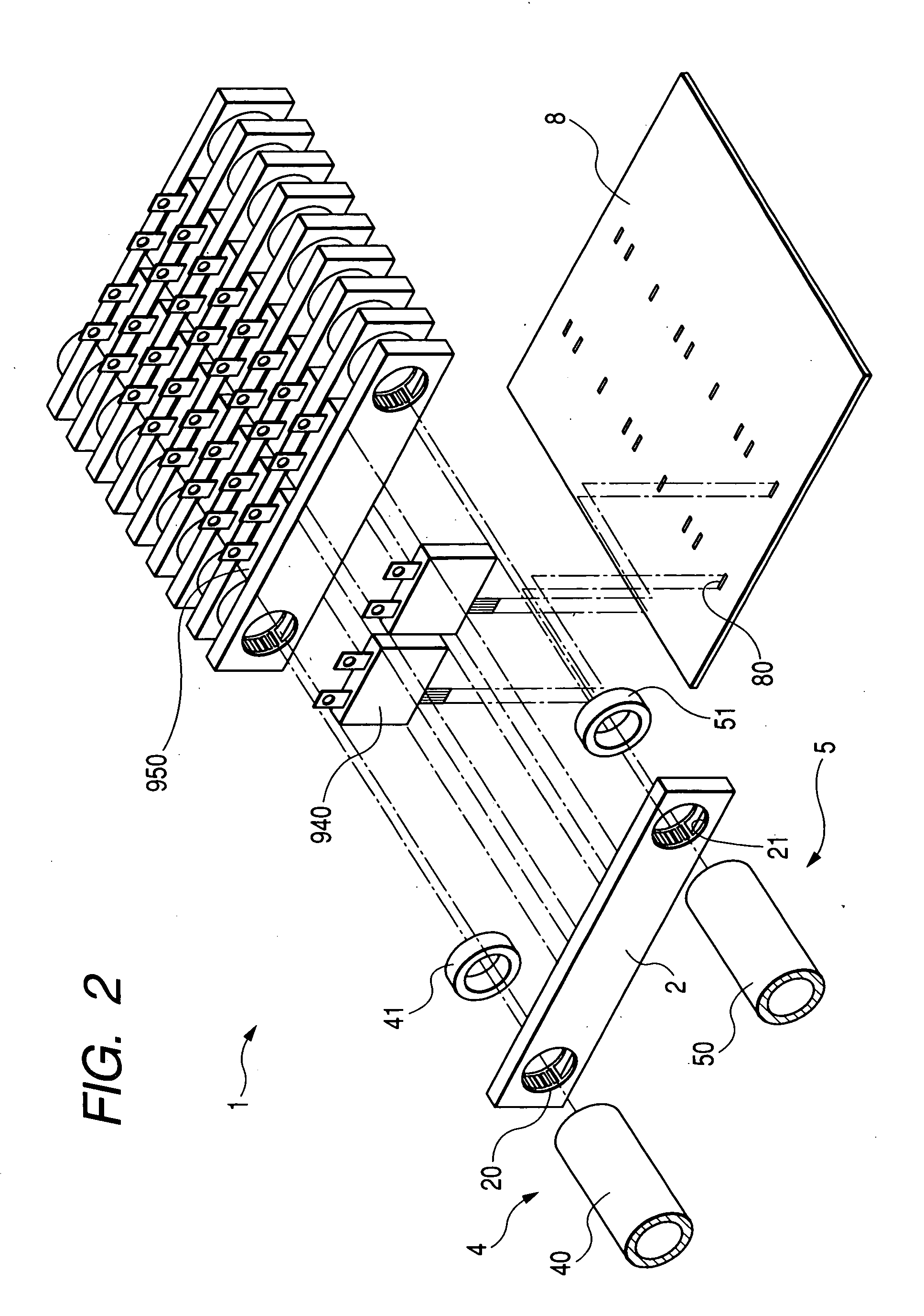
[0092]FIG. 8 shows a partly exploded perspective view of a power stack 1a in accordance with this embodiment. The components or portions corresponding to those shown in FIG. 2 are denoted by the same reference numerals. FIG. 9 shows a perspective view of an assembled condition of this power stack 1a. The components or portions corresponding to those shown in FIG. 3 are denoted by the same reference numerals. FIG. 10 shows a cross-sectional view of this power stack 1a. The components or portions corresponding to those shown in FIG. 6 are denoted by the same reference numerals.

[0093] For example, as understood from the comparison between FIG. 10 and FIG. 6, the power stack la of this embodiment has a main inlet pipe 40 and a main...

third embodiment

[0101] The third embodiment is different from the second embodiment in the layout of the first switching modules, the second switching modules, and the converter switching modules. Hereinafter, this embodiment is explained only about the differences.

[0102]FIG. 12 shows a schematic plan view of a power stack 1b in accordance with this embodiment. The components or portions corresponding to those shown in FIG. 11 are denoted by the same reference numerals and the same hatching. As shown in the drawing, all of the second switching module 950 (twelve in total) are disposed at the downstream side of the cooling pipes 2 in the flow direction of LLC (refer to FIG. 10). The converter switching modules 931 are disposed at the upstream side of six second switching modules 950 disposed adjacently to the electric reactor 930. Furthermore, the first switching modules 940 are disposed at the upstream side of the remaining six second switching modules 950 disposed far from the electric reactor 93...


PUM


Abstract

A power stack includes cooling pipes and semiconductor modules which are alternately laminated. Each cooling pipe includes an inside space dissected into cooling passages in which coolant flows. Both surfaces of the semiconductor module in a laminating direction are brought into contact with surfaces of neighboring cooling pipes. The semiconductor modules are classified into a plurality of groups mutually differentiated in their heat generation rates. And, any two semiconductor modules belonging to the same group having the highest heat generation rate are spaced from each other so that a cooling pipe is not sandwiched between these semiconductor modules in the laminating direction.

Description

CROSS-REFERENCE TO RELATED APPLICATION [0001] This application is based upon and claims the benefit of priority from earlier Japanese Patent Application No. 2004-147691 filed on May 18, 2004 so that the description of which is incorporated herein by reference. BACKGROUND OF THE INVENTION [0002] The present invention relates to a power stack which is preferable used as a driving apparatus for an automotive electric rotary machine. [0003] For example, the following prior art documents 1 to 4 respectively disclose a power stack including cooling members and semiconductor elements alternately laminated, according to which the semiconductor element is sandwiched between a pair of cooling members disposed in the laminating direction. The heat generated from the semiconductor element is absorbed by these cooling members. Therefore, the power stacks disclosed in the prior art documents 1 to 4 can prevent thermal breakdown of semiconductor elements. [0004] 1: Japanese Patent Application Laid...

Claims


Application Information

Patent Timeline
Patent Type & Authority Applications(United States)
IPC IPC(8): H01L23/34H01L23/40H01L23/473H02M7/00H05K7/14H05K7/20
CPCH02M7/003H05K7/20927H01L2924/0002H01L2924/00
Inventor YASUI, HIDEHIKOISHIYAMA, HIROSHI
Owner DENSO CORP
Why Eureka
Try Eureka