Helical optical pulse stretcher

a technology of optical pulses and stretchers, which is applied in the direction of printers, lasers, instruments, etc., can solve the problems of limited space available for projection optical systems with lithographic tools, difficult design of optical components used in microlithography, and frequent replacement of optical components

Inactive Publication Date: 2005-11-24
ASML HLDG NV
View PDF1 Cites 14 Cited by
  • Summary
  • Abstract
  • Description
  • Claims
  • Application Information

AI Technical Summary

Benefits of technology

[0010] The present invention is directed to a helical optical pulse stretcher that...

Problems solved by technology

A difficulty in designing optical components used in microlithography is caused by the high power density involved during exposure.
The high intensity pulses, over time, damage optical components, such as lenses used in the projection optics, requiring frequent replacement of these...

Method used


Image

  • Helical optical pulse stretcher
  • Helical optical pulse stretcher
  • Helical optical pulse stretcher

Examples


Embodiment Construction

[0020] While specific configurations and arrangements are discussed, it should be understood that this is done for illustrative purposes only. A person skilled in the pertinent art will recognize that other configurations and arrangements can be used without departing from the spirit and scope of the present invention. It will be apparent to a person skilled in the pertinent art that this invention can also be employed in a variety of other applications.

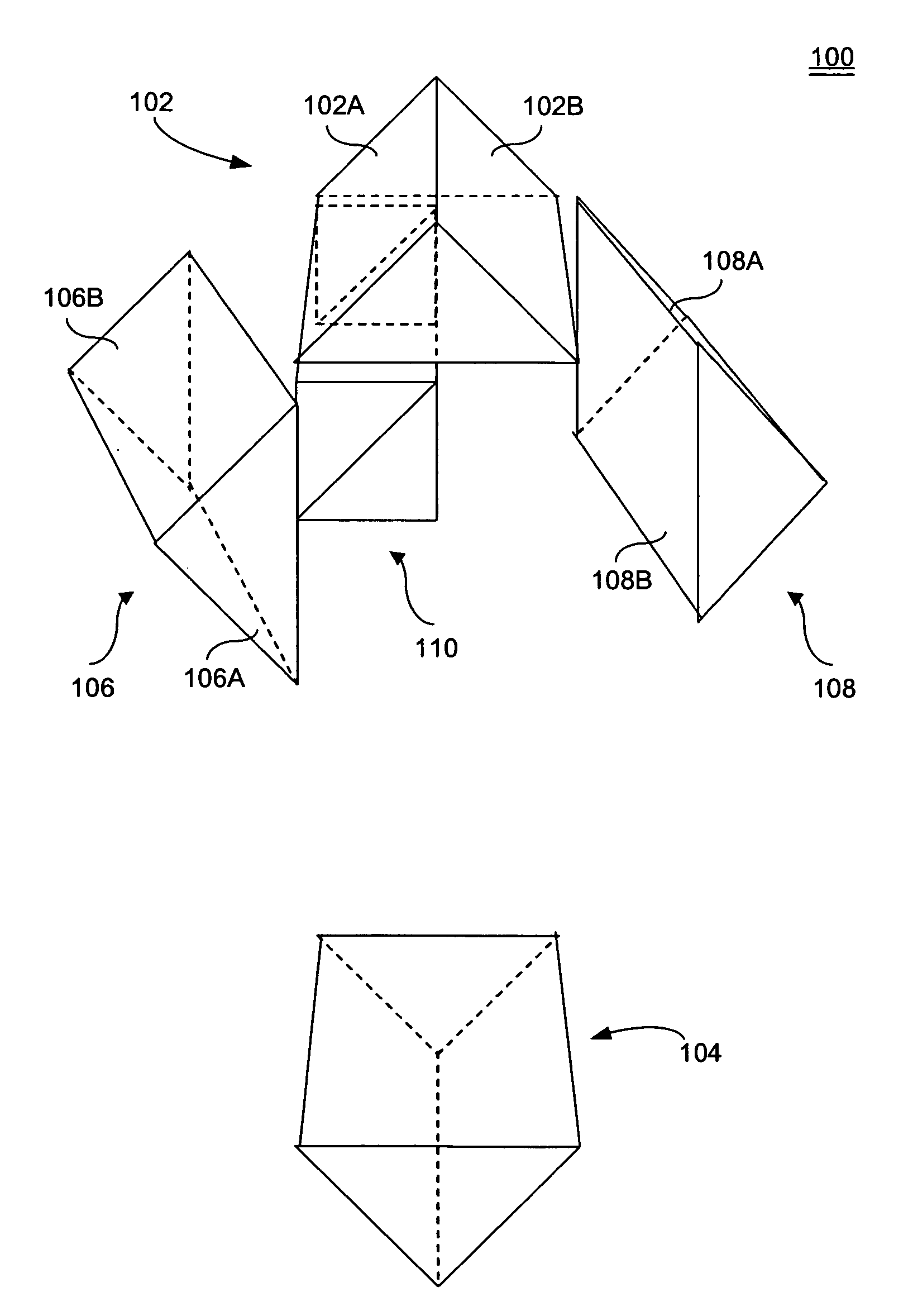
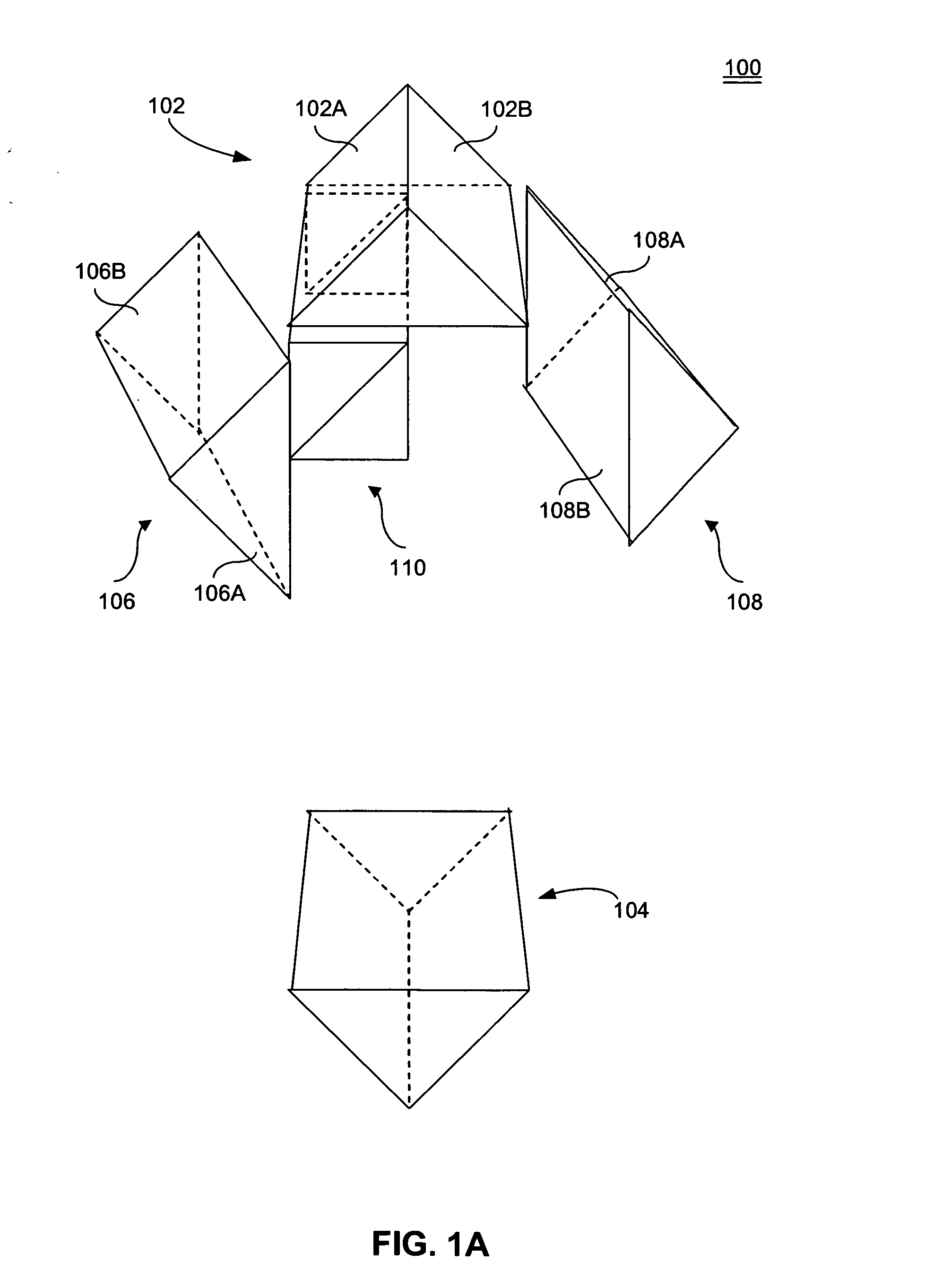
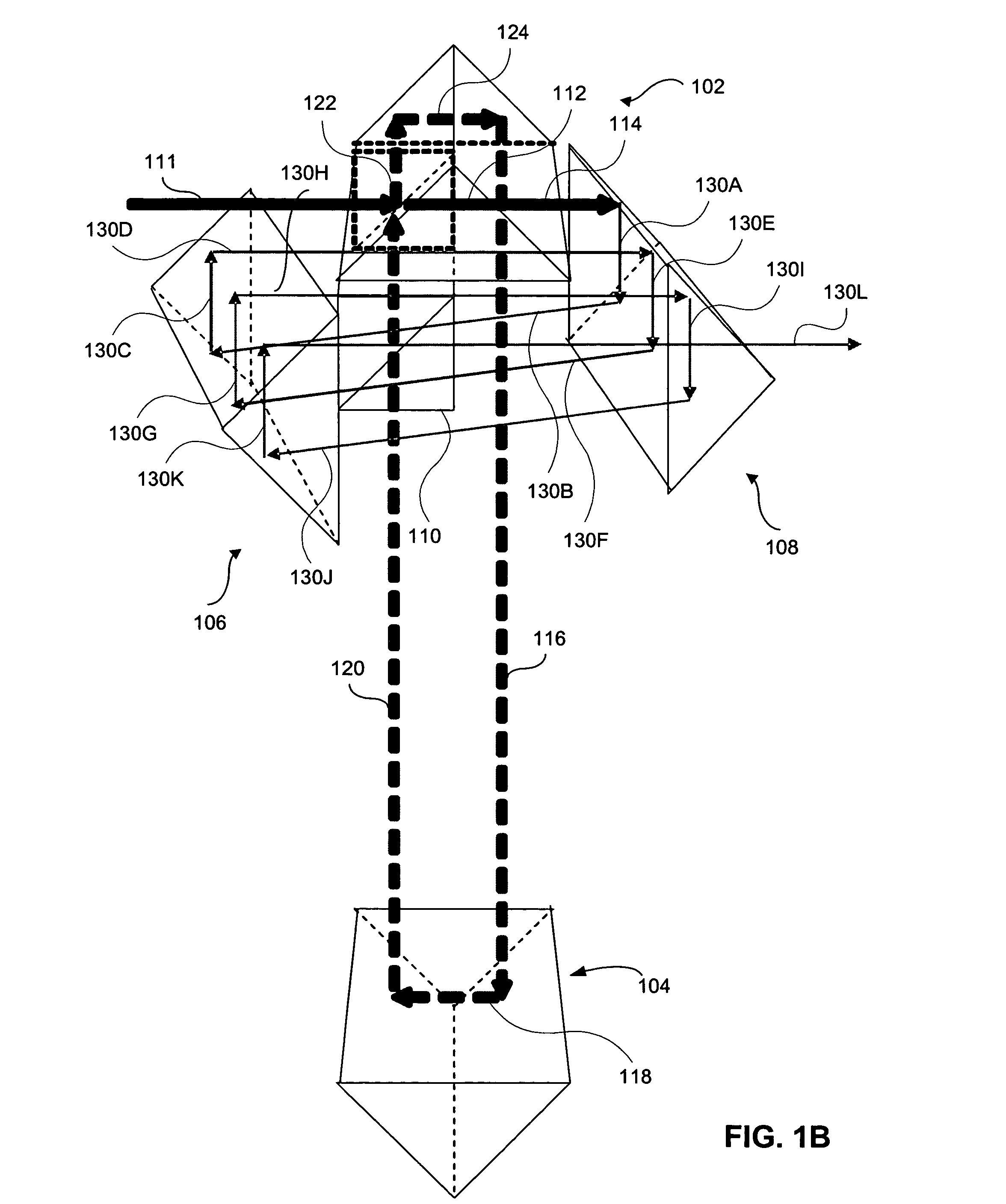
[0021]FIGS. 1A and 1B show an exemplary embodiment of the present invention. For clarity, FIG. 1A shows only the optical components, while FIG. 1B shows the same components with the propagating light beams added and labeled. In the discussion below, the sense of direction (i.e., left, right, up, down) is for illustrative use only, and is not intended to limit the present invention.

[0022]FIG. 1A illustrates a perspective view of an exemplary pulse stretcher of the present invention. Shown in FIG. 1A are the following components: a p...


PUM


Abstract

A pulse stretcher includes a single pass pulse stretcher. An optical system is arranged around the single pass pulse stretcher. A beam enters the single pass stretcher and is reflected in a helical path using the optical system for multiple passes through the single pass pulse stretcher. The single pass pulse stretcher can include two 90° prisms, with a beam splitter located therebetween. The optical system can include first and second prisms. At least one of the first and second prisms can be a roof prism. The first and second prisms can have at least one surface oriented so as to direct the beam into the helical path. The optical system can have at least one mirror, or a plurality of mirrors.

Description

BACKGROUND OF THE INVENTION [0001] 1. Field of the Invention [0002] The present invention relates to pulse stretchers, and more particularly, to helical pulse stretchers for use in lithography applications. [0003] 2. Related Art [0004] Lithography is a process used to create features on the surface of substrates. Such substrates can include those used in the manufacture of flat panel displays (e.g., liquid crystal displays), circuit boards, various integrated circuits, and the like. A frequently used substrate for such applications is a semiconductor wafer or glass substrate. [0005] During lithography, a wafer, which is disposed on a wafer stage, is exposed to an image projected onto the surface of the wafer by exposure optics located within a lithography apparatus. While exposure optics are used in the case of photolithography, a different type of exposure apparatus can be used depending on the particular application. For example, x-ray, ion, electron, or photon lithography each ca...

Claims


Application Information

Patent Timeline
IPC IPC(8): G03F7/20H01L21/027G02B5/04H01S3/00H01S3/08H01S3/13
CPCG03F7/70041G03F7/70058Y10S372/70H01S3/0057G03F7/7055
Inventor ALBERT, MICHAEL M.
Owner ASML HLDG NV
Why Eureka
Try Eureka