Surface shape recognition sensor

a surface shape and sensor technology, applied in the field of biometric recognition, can solve the problems of card missing or theft at high probability, and achieve the effect of accurate biometric recognition, avoiding any increase in device size, and easy implementation of on-chip device formation

Inactive Publication Date: 2005-11-24
NIPPON TELEGRAPH & TELEPHONE CORP
View PDF4 Cites 32 Cited by
  • Summary
  • Abstract
  • Description
  • Claims
  • Application Information

AI Technical Summary

Benefits of technology

[0036] According to the present invention, a first detection element having a first detection electrode connected to a surface shape detection unit and a second detection electrode connected to a common potential, and a second detection element having a first detection electrode connected to the surface shape detection unit and a second detection electrode connected to a biometric recognition unit are arranged. The surface shape detection unit detects the surface shape on the basis of individual capacitances obtained from the first and second detection elements. The biometric recognition unit executes biometric recognition on the basis of a signal corresponding to the impedance of an object connected between the second detection electrode of the second detection element and the second detection electrode of the first detection element. With this arrangement, accurate biometric recognition can be executed while suppressing a potential variation induced to the object. In addition, on-chip device formation can easily be implemented by avoiding any increase in device size due to addition of a detection electrode.
[0037] According to the present invention, the capacitance detection units for surface shape detection are arranged in a matrix together with the detection elements. In place of one of the capacitance detection units, the impedance detection unit for biometric recognition is arranged together with the detection element as a pair. With this arrangement, the interconnection which connects the detection element for biometric recognition to the impedance detection unit to drive the detection element can be very short. Since the parasitic capacitance or noise of this interconnection can be reduced, the impedance of the object can accurately be detected. Hence, a high determination accuracy can be obtained in biometric recognition.
[0038] In the impedance detection unit, a predetermined supply signal is applied to the detection element. A signal whose phase and amplitudes have changed in accordance with the impedance of the object is acquired as a response signal. Waveform information containing the phase or amplitude representing the waveform of the response signal is detected and output as a detection signal. Determination is done by the biometric determination unit on the basis of determination data obtained by A / D-converting the detection signal. For example, a resistive element or capacitive element which requires a large area is not always necessary, unlike the prior art. Waveform information representing the impedance unique to the object can be detected in detail by a very simple circuit arrangement such as a general comparator and logic circuit. Hence, size reduction of the surface shape recognition sensor device and on-chip device formation can easily be implemented. In addition, the external component such as a resistive element or capacitive element is unnecessary. Since any decrease in security level caused by the external component can be avoided, sufficient security can be obtained.

Problems solved by technology

However, the cards can be missing or stolen at high probability.

Method used


Image

  • Surface shape recognition sensor
  • Surface shape recognition sensor
  • Surface shape recognition sensor

Examples


first embodiment

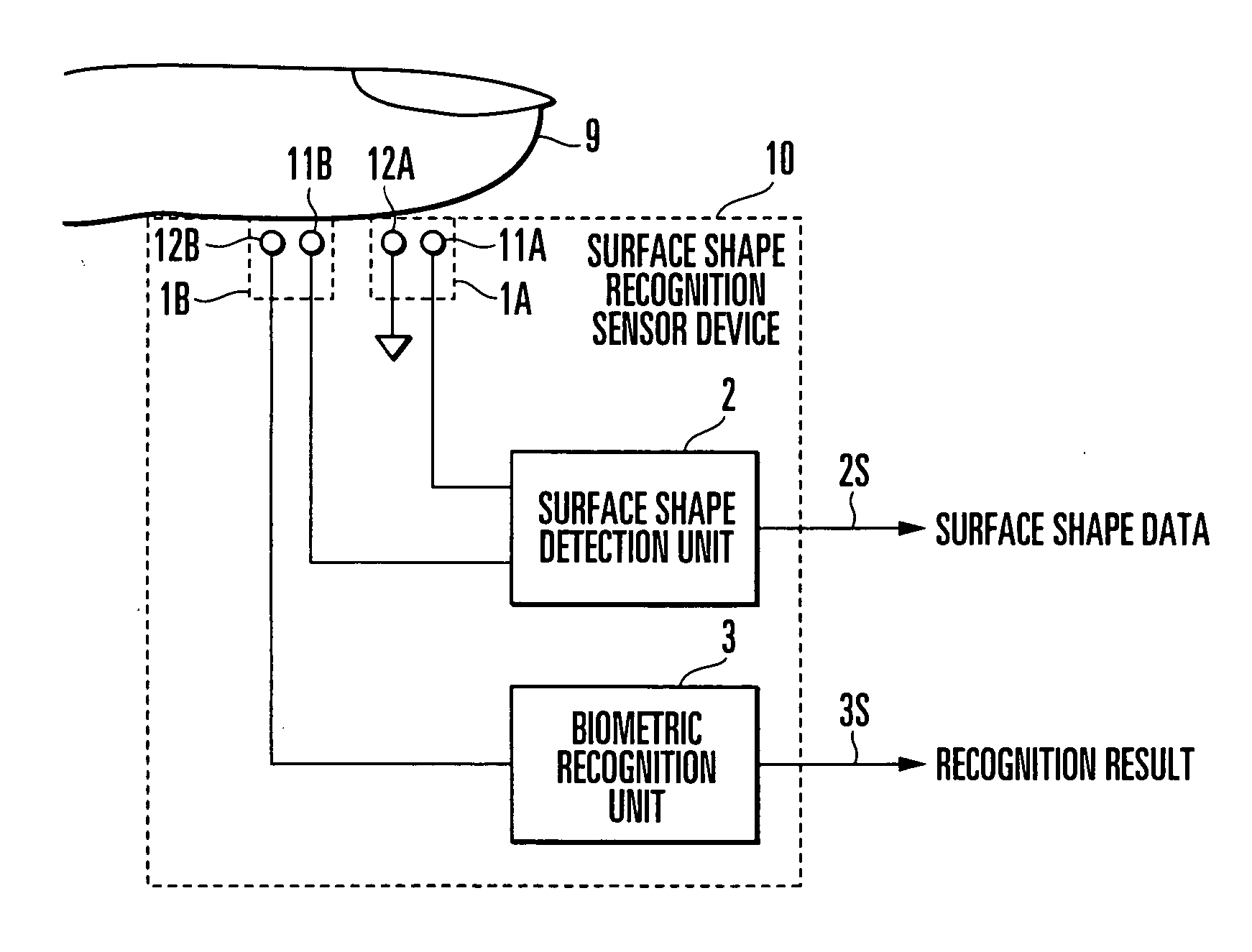
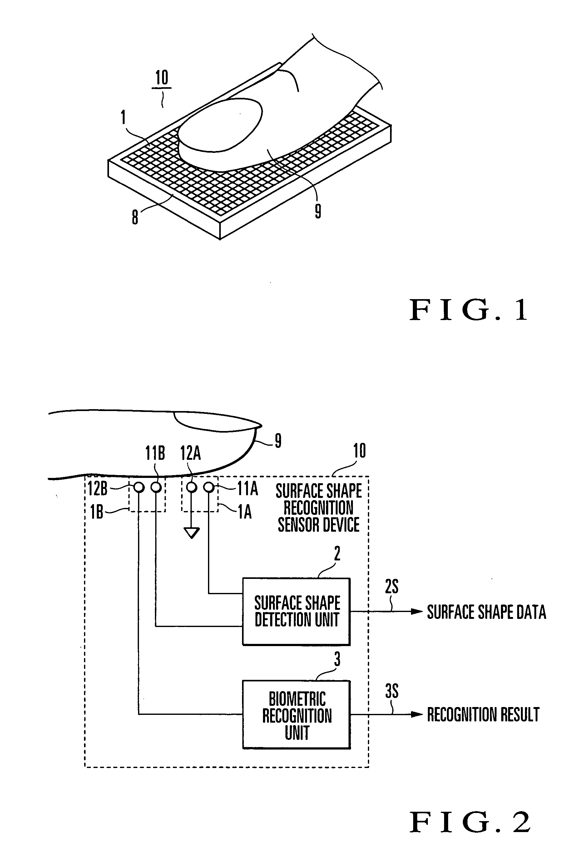
[0067] A surface shape recognition sensor device according to the first embodiment of the present invention will be described next with reference to FIG. 2. FIG. 2 is a block diagram showing the arrangement of the surface shape recognition sensor device according to the first embodiment of the present invention.

[0068] A surface shape recognition sensor device 10 includes detection elements 1A and 1B, surface shape detection unit 2, and biometric recognition unit 3.

[0069] The detection element 1A has a detection electrode 11A which forms an electrostatic capacitance with respect to an object 9 through an insulating film, and a detection electrode 12A which comes into electrical contact with the object 9. The detection electrode 11A is connected to the surface shape detection unit 2. The detection electrode 12A is connected to a common potential such as a ground potential. The common potential is supplied from a predetermined supply circuit unit (not shown) such as a power supply ci...

second embodiment

[0105] A surface shape recognition sensor device according to the second embodiment of the present invention will be described next with reference to FIG. 9. FIG. 9 is a block diagram showing the arrangement of the surface shape recognition sensor device according to the second embodiment of the present invention.

[0106] In a surface shape recognition sensor device 10, a detection element 1C is arranged between a detection element 1A and a detection element 1B, unlike the above-described first embodiment (FIG. 2). The remaining parts are the same as in the above-described first embodiment. The same reference numerals as in FIG. 2 denote the same or similar parts in FIG. 9.

[0107] The detection element 1C has a detection electrode 11C which forms an electrostatic capacitance with respect to an object 9 through an insulating film, and a detection electrode 12C which comes into electrical contact with the object 9, like the above-described detection elements 1A and 1B. The detection el...

third embodiment

[0118] A surface shape recognition sensor device according to the third embodiment of the present invention will be described next with reference to FIG. 11. FIG. 11 is a block diagram showing the arrangement of the surface shape recognition sensor device according to the third embodiment of the present invention.

[0119] In a surface shape recognition sensor device 10, a switch 4C is arranged between the common potential and a detection electrode 12C of a detection element 1C, unlike the above-described second embodiment (FIG. 9). The remaining parts are the same as in the above-described second embodiment. The same reference numerals as in FIG. 9 denote the same or similar parts in FIG. 11.

[0120] When a surface shape detection unit 2 executes the surface shape detection operation, the switch 4C is short-circuited to apply the common potential to the detection electrode 12C of the detection element 1C. When a biometric recognition unit 3 executes the biometric recognition operation...


PUM


Abstract

A detection element (1A) having a detection electrode (11A) connected to a surface shape detection unit (2) and a detection electrode (12A) connected to a common potential, and a detection element (1B) having a detection electrode (11B) connected to the surface shape detection unit (2) and a detection electrode (12B) connected to a biometric recognition unit (3) are arranged. The surface shape detection unit (2) outputs a signal representing the three-dimensional pattern of the surface shape corresponding to the contact portion to each detection element on the basis of individual capacitances obtained from the detection elements (1A, 1B). The biometric recognition unit (3) determines whether an object (9) is a living body, on the basis of a signal corresponding to the impedance of the object (9) connected between the detection electrode (12B) of the detection element (1B) and the detection electrode (12A) of the detection element (1A).

Description

TECHNICAL FIELD [0001] The present invention relates to a surface shape recognition sensor device and, more particularly, to a biometric recognition technique for recognizing a person by detecting biometric information such as a fingerprint from an object. BACKGROUND ART [0002] As the information-oriented society becomes more advanced, technologies for security protection of information processing systems have been developed. For example, ID cards are conventionally used to control access to computer rooms. However, the cards can be missing or stolen at high probability. To prevent this, introduction of personal recognition systems is starting, in which the fingerprint or the like of each person is registered in advance, and the fingerprint unique to each person is collated when he / she accesses the room, instead of using the ID cards. [0003] Such a personal recognition system sometimes passes, e.g., a replica of a registered fingerprint. Hence, the personal recognition system must a...

Claims


Application Information

Patent Timeline
Patent Type & Authority Applications(United States)
IPC IPC(8): G01B7/28G06K9/00
CPCG06K9/0012G06K9/0002G06V40/1306G06V40/1394
Inventor SHIMAMURA, TOSHISHIGEMORIMURA, HIROKISHIGEMATSU, SATOSHISATO, NORIOURANO, MASAMIMACHIDA, KATSUYUKI
Owner NIPPON TELEGRAPH & TELEPHONE CORP
Why Eureka
Try Eureka