
Annealing modified interface in organic light emitting devices

a light-emitting device and modified interface technology, applied in the direction of discharge tube/lamp details, discharge tube luminescnet screens, transportation and packaging, etc., can solve the problem of more difficult to tune inorganic emissive materials

Inactive Publication Date: 2005-11-24
KWONG RAYMOND
View PDF10 Cites 0 Cited by
  • Summary
  • Abstract
  • Description
  • Claims
  • Application Information

AI Technical Summary

Benefits of technology

[0017] A method of fabricating an organic light emitting device is provided. A substrate having a first conductive layer disposed thereon is obtained. A first small molecule organic layer is deposited over the conductive layer. A second small molecule organic layer is deposited on top of the first small molecule organic layer. The first and second small molecule organic layers are annealed. The annealing is at a temperature such that either (1) there is no significant crystallization of the first and second small molecule organic layers, or (2) the temperature does not exceed the glass transition temperature of either the first or the second small molecule organic layers. A second conductive layer is deposited over the second small molecule organic layer after annealing. A third small molecule organic layer may be deposited either before or after the annealing. In one embodiment, either the first or second small molecule organic layers may be replaced with a polymer layer.

Problems solved by technology

In addition, the wavelength at which an organic emissive layer emits light may generally be readily tuned with appropriate dopants, while it may be more difficult to tune inorganic emissive materials.

Method used


Image

  • Annealing modified interface in organic light emitting devices
  • Annealing modified interface in organic light emitting devices
  • Annealing modified interface in organic light emitting devices

Examples


example 1

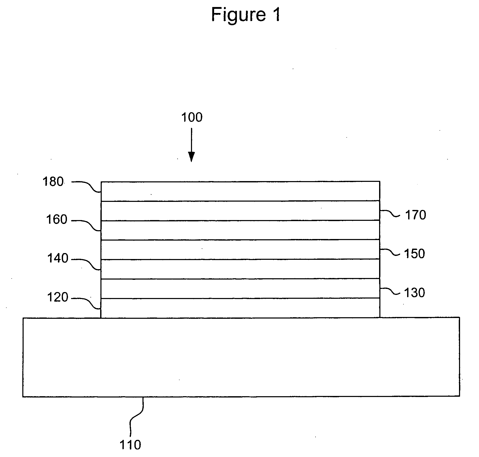
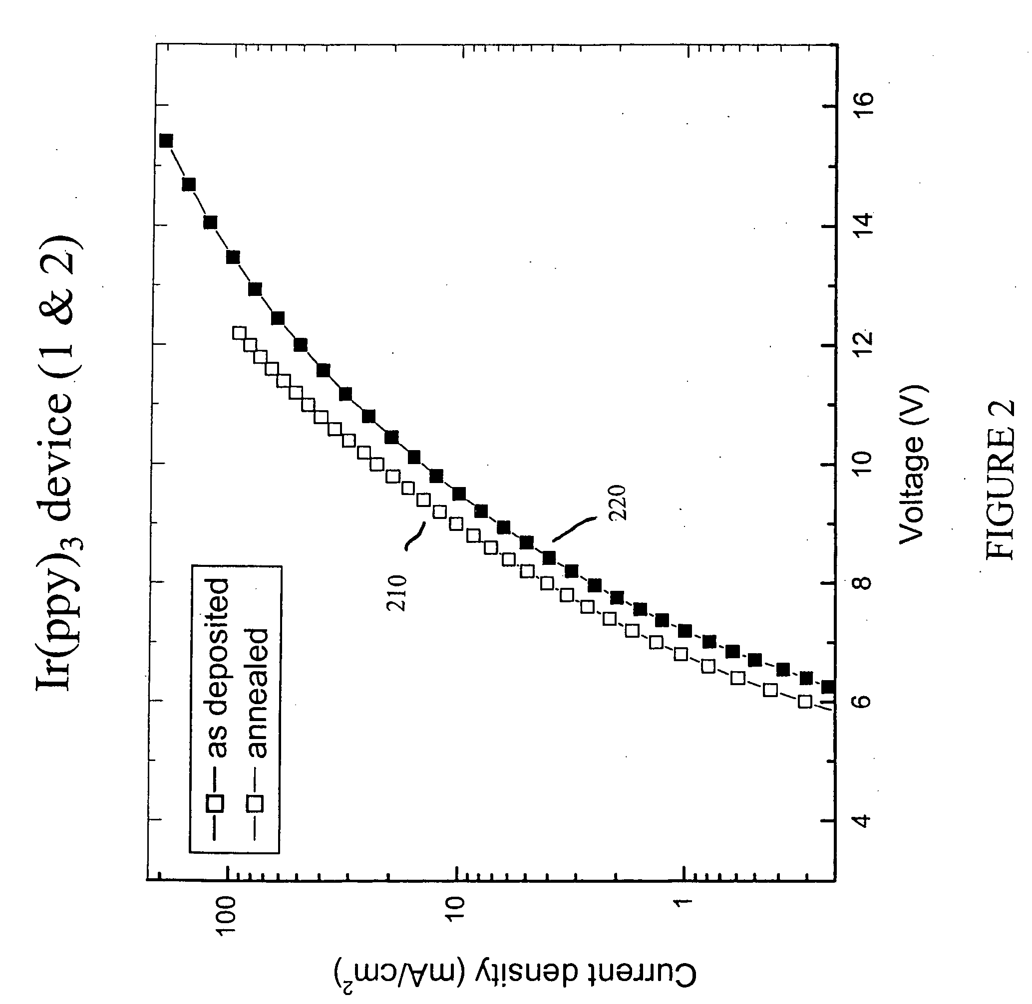
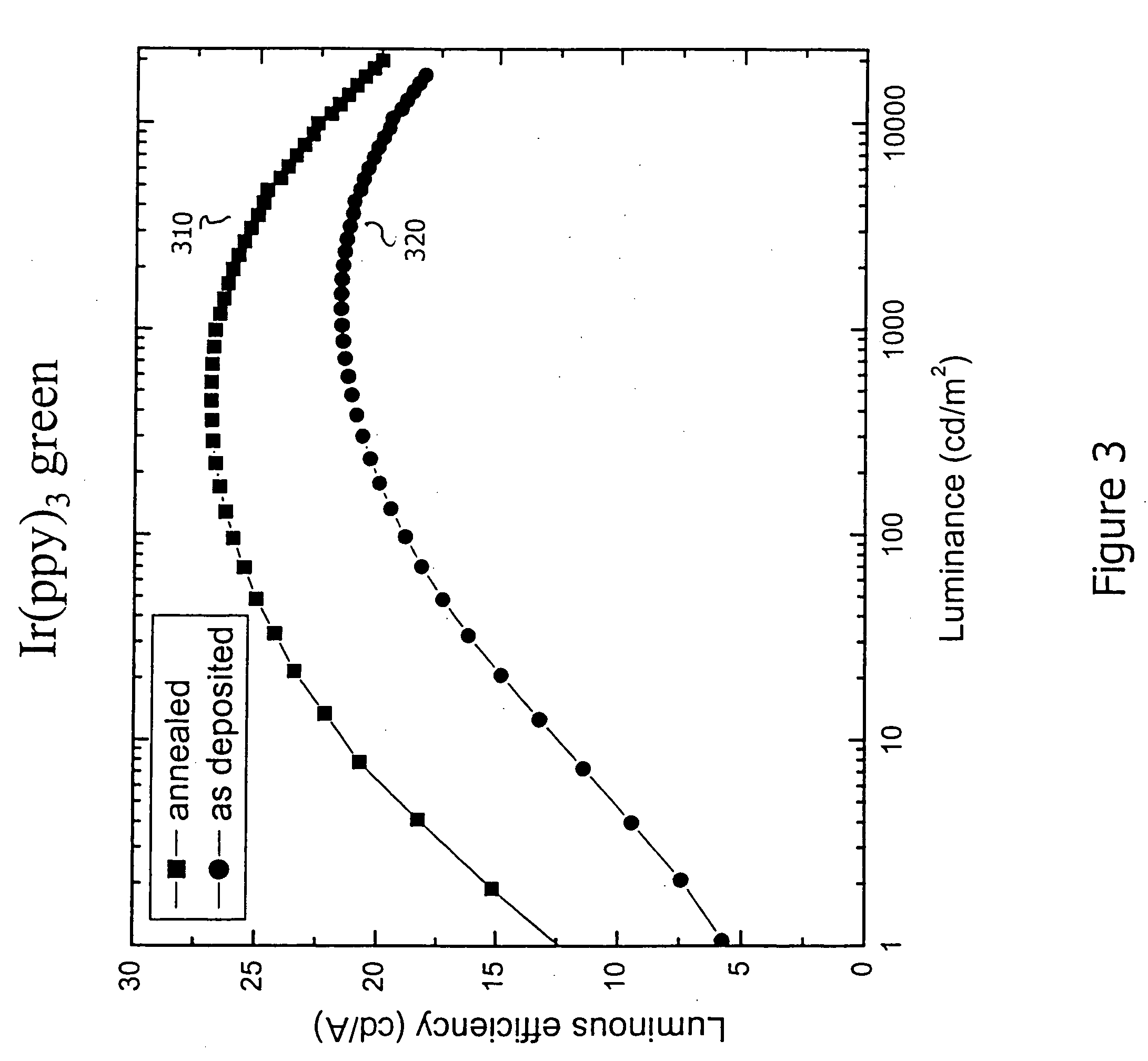
[0039] The following materials were deposited, in sequence: CuPc (100 Å), NPD (150 Å). The CuPc and NPD were annealed at 80 C for one hour, and the device was then cooled to room temperature. After annealing, the following materials were deposited in sequence: NPD (50 Å), CBP:Ir(Ppy)3 (300 Å), BAlq (100 Å), Alq3 (400 Å), LiF (10 Å), Al (1000 Å). All steps, including annealing, were performed in situ without removing the device (“device 1”) from vacuum. The Ir(Ppy)3 emissive layer of device 1 emits green light.

example 2

[0040] The following materials were deposited, in sequence: CuPc (100 Å), NPD (300 Å), CBP:Ir(Ppy)3 (300 Å), BAlq (10 Å), Alq3 (400 Å), LiF (10 Å), Al (1000 Å). All steps were performed in situ without removing the device from vacuum. The resultant device (“device 2”) has the same layered structure as device 1, except that there was no annealing during the fabrication of device 2. As with device 1, device 2 is designed to emit green light.

example 3

[0041] A device (“device 3”) was fabricated using the method described in Example 1. However, after depositing NPD (150 Å), 300 Å of CBP:BTPIr was deposited instead of 300 Å of CBP:Ir(Ppy)3. As a result, device 3 is designed to emit red light.


PUM


Abstract

A method of fabricating an organic light emitting device is provided. A substrate having a first conductive layer disposed thereon is obtained. A first small molecule organic layer is deposited over the conductive layer. A second small molecule organic layer is deposited on top of the first small molecule organic layer. The first and second small molecule organic layers are annealed. The annealing is at a temperature such that either (1) there is no significant crystallization of the first and second small molecule organic layers, or (2) the temperature does not exceed the glass transition temperature of either the first or the second small molecule organic layers. A second conductive layer is deposited over the second small molecule organic layer after annealing. A third small molecule organic layer may be deposited either before or after the annealing. In one embodiment, either the first or second small molecule organic layers may be replaced with a polymer layer.

Description

FIELD OF THE INVENTION [0001] The present invention relates to the field of organic light emitting devices, and more particularly to the fabrication of the organic layers used in such devices. BACKGROUND OF THE INVENTION [0002] Organic light emitting devices (OLEDs) are becoming increasingly desirable for a number of reasons. Many of the materials used to make such devices are relatively inexpensive, so organic light emitting devices have the potential for cost advantages over inorganic devices. In addition, the inherent properties of organic materials, such as their flexibility, may make them well suited for particular applications such as fabrication on a flexible substrate. In addition, the wavelength at which an organic emissive layer emits light may generally be readily tuned with appropriate dopants, while it may be more difficult to tune inorganic emissive materials. [0003] OLEDs make use of thin organic films that emit light when voltage is applied across the device. OLEDs a...

Claims


Application Information

Patent Timeline
Patent Type & Authority Applications(United States)
IPC IPC(8): H01L51/50H01L51/56
CPCH01L51/5012H01L51/5016Y10T428/24942H01L51/56H01L51/5048H10K50/11H10K2101/10H10K50/14H10K71/40H10K71/00
Inventor KWONG, RAYMOND
Owner KWONG RAYMOND
Learn More