

Method of manufacturing semiconductor device
- Summary
- Abstract
- Description
- Claims
- Application Information
AI Technical Summary
Benefits of technology
Problems solved by technology
Method used
Image

Examples
embodiment mode 1
[Embodiment Mode 1]
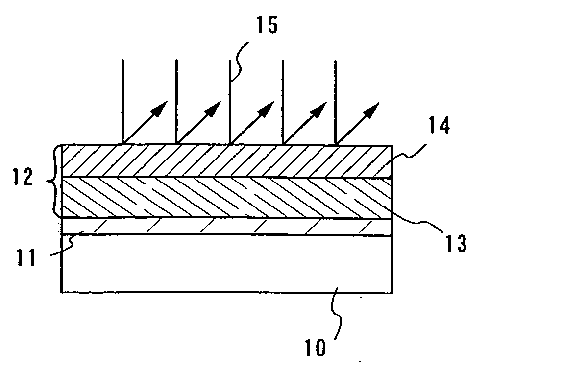
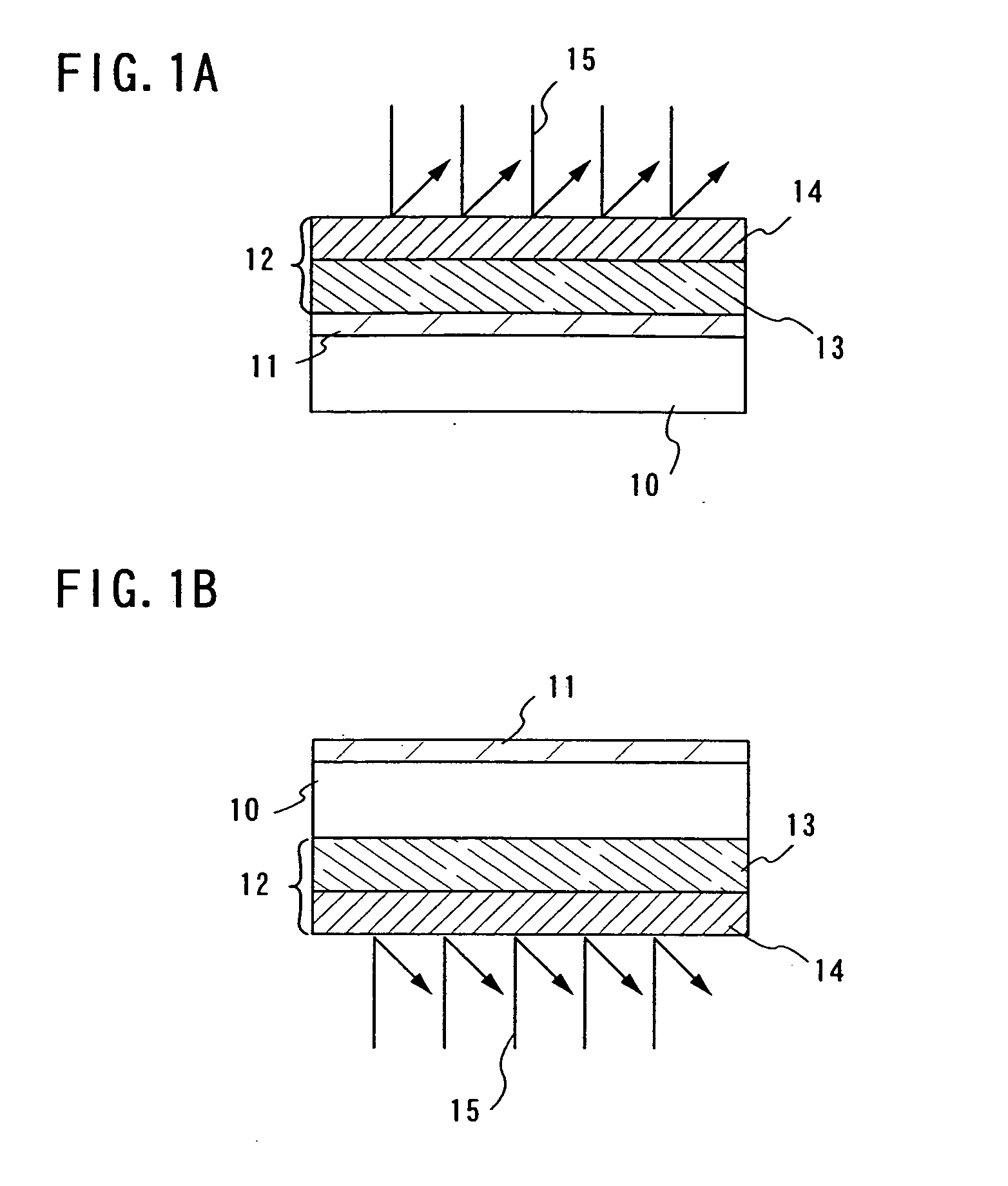
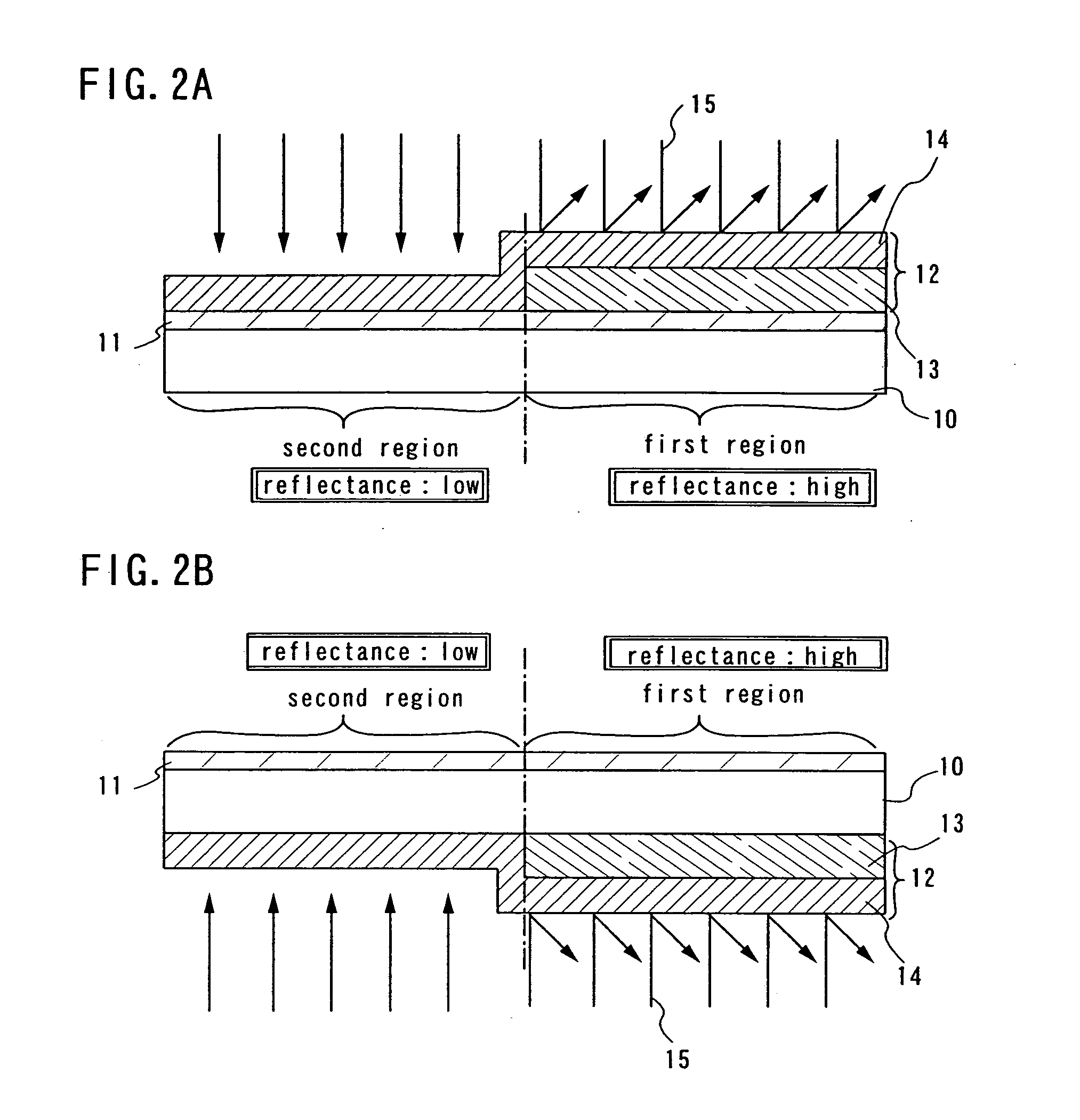
In Embodiment Mode 1, a structure of a mask formed over an amorphous semiconductor film will be described.
In FIG. 1A, a mask 12 is formed over a top surface of a substrate 10 having an insulated surface while interposing an amorphous semiconductor film 11 therebetween. The mask 12 is composed of a first material 13 and a second material 14. It is preferable that the first material be formed of a material having lower refractive index, and the second material be formed of a material having higher refractive index than that of the first material. For example, the first material 13 may be formed of a silicon oxynitride (SiON) film, whereas the second material 14 may be formed of a silicon nitride oxide (SiNO) film. Further, for instance, the silicon oxynitride (SiON) film may be formed by plasma-CVD under a condition in which SiH4 and N2O are used as material gases; the pressure is 0.3 Torr; RF power is 150 W; RF frequency is 60 MHz; and the substrate temperature ...
embodiment mode 2
[Embodiment Mode 2]
Embodiment Mode 2 will describe steps for manufacturing a thin film transistor including a laser crystallization step with use of a mask, and steps for manufacturing a display device including a light emitting element typified by an organic light emitting element for each pixel.
Firstly, as illustrated in FIG. 3A, base films including laminated films 101a and 101b are formed over a top surface of a substrate 100 having an insulated surface. As the substrate 100, for example, a glass substrate such as a barium-borosilicate glass and an alumino-borosilicate glass, a quartz substrate, an SUS substrate and the like can be used. In addition, although a substrate formed of flexible synthetic resin such as acryl and plastic typified by PET, PES, and PEN generally tends to be inferior in heat resistance as compared with the other substrates, the substrate made of flexible synthetic resin can be used when it can withstand the processing temperature in the manufacturing s...
embodiment mode 3
[Embodiment Mode 3]
Embodiment Mode 3 will describe a case of crystallizing an amorphous semiconductor film by doping a metal element thereinto so as to form a crystalline semiconductor film in the thin film transistor of the driver circuit portion as described in Embodiment Mode 2.
In FIG. 4A, the laminated films 106a and 106b are formed as a mask in a pixel portion in the same manner as FIG. 3A. While covering the pixel portion with the mask, a metal element is added over the surface of the substrate. The addition of the metal element indicates that the surface of the amorphous semiconductor film 104 is coated with the metal element so as to promote the crystallization of the amorphous semiconductor film. The amorphous semiconductor film can be crystallized at low temperatures by addition the metal element thereon.
For instance, Ni solution (including Ni aqueous solution and Ni acetate solution) is applied on the amorphous semiconductor film 104 by spin coating, dipping, and the...
PUM
 Abstract
Description
Claims
Application Information